DS3170N+ Maxim Integrated Products, DS3170N+ Datasheet - Page 34
DS3170N+
Manufacturer Part Number
DS3170N+
Description
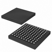
IC TXRX DS3/E3 100-CSBGA
Manufacturer
Maxim Integrated Products
Datasheet
1.DS3170.pdf
(230 pages)
Specifications of DS3170N+
Function
Single-Chip Transceiver
Interface
DS3, E3
Number Of Circuits
1
Voltage - Supply
3.135 V ~ 3.465 V
Current - Supply
120mA
Operating Temperature
-40°C ~ 85°C
Mounting Type
Surface Mount
Package / Case
100-LBGA
Includes
DS3 Framers, E3 Framers, HDLC Controller, On-Chip BERTs
Lead Free Status / RoHS Status
Lead free / RoHS Compliant
Power (watts)
-


CS
RD /
DS
WR /
R/W
RDY
INT
MODE
WIDTH
SPI
GPIO1
GPIO2
GPIO3
GPIO4
GPIO5
GPIO6
GPIO7
PIN NAME
TYPE
Oz
Oz
IO
IO
IO
IO
IO
IO
IO
I
I
I
I
I
I
address systems. When it is high the address is fed through the address latch to the
internal logic. When it transitions to low, the address is latched and held internally
until the signal goes back high. ALE should be tied high for nonmultiplexed address
systems.
Chip Select (active low)
CS: This signal must be low during all accesses to the registers
Read Strobe (active low) / Data Strobe (active low)
RD: Read Strobe mode (MODE=0):
DS: Data Strobe mode (MODE=1):
Write Strobe (active low) / R/W Select
WR: Write Strobe mode (MODE=0):
R/W: Data Strobe mode (MODE=1):
Ready handshake (active low)
RDY: This ready signal is driven low when the current read or write cycle can
progress. When the current read or write cycle is not ready it is driven high. When
device is not selected it is not driven. Not driven when RST=0 or CS=1.
Interrupt (active low)
INT: This interrupt signal is driven low when an event is detected on any of the
enabled interrupt sources in any of the register banks. When there are no active and
enabled interrupt sources, the pin can be programmed to either drive high or not drive
high. The reset default is to not drive high when there are no active and enabled
interrupt source. All interrupt sources are disabled when RST =0 and they must be
programmed to be enabled.
Not driven when RST=0.
Mode select RD/WR or DS strobe mode
MODE: 1 = Data Strobe Mode, 0 = Read/Write Strobe Mode
Data bus width select 8 or 16-bit interface
WIDTH: 1 = 16-bits, 0 = 8 bits
SPI Serial Bus Mode Select
SPI: 1 = SPI Serial Bus Mode, 0 = Parallel Bus Mode
General Purpose IO 1
GPIO1: This signal is configured to be a general purpose IO pin, or an alarm output
signal.
General Purpose IO 2
GPIO2: This signal is configured to be a general purpose IO pin, or the 8KREFO
output signal, or an alarm output signal.
General Purpose IO 3
GPIO3: This signal is configured to be a general purpose IO pin.
General Purpose IO 4
GPIO4: This signal is configured to be a general purpose IO pin, or the 8KREFI input
signal. When configured for 8KREFI mode the signal frequency should be 8,000 Hz
+/- 500 ppm and about 50% duty cycle.
General Purpose IO 5
GPIO5: This signal is configured to be a general purpose IO pin, or an alarm output
signal.
General Purpose IO 6
GPIO6: This signal is configured to be a general purpose IO pin, or the TMEI input
signal. When configured for TMEI input, the signal low time and high time must be
greater than 500 nsec.
General Purpose IO 7
RD is low during a register read.
DS is low during either a register read or a write.
WR is low during a register write.
R/W is high during a register read cycle, and low during a register write cycle.
34 of 230
Misc I/O
PIN DESCRIPTION
DS3170 DS3/E3 Single-Chip Transceiver
Related parts for DS3170N+
Image
Part Number
Description
Manufacturer
Datasheet
Request
R

Part Number:
Description:
IC TXRX DS3/E3 100-CSBGA
Manufacturer:
Maxim Integrated Products
Datasheet:

Part Number:
Description:
Network Controller & Processor ICs DS3-E3 Single-Chip T ransceiver T3-E3 Fra
Manufacturer:
Maxim Integrated Products
Datasheet:
Part Number:
Description:
MAX7528KCWPMaxim Integrated Products [CMOS Dual 8-Bit Buffered Multiplying DACs]
Manufacturer:
Maxim Integrated Products
Datasheet:
Part Number:
Description:
Single +5V, fully integrated, 1.25Gbps laser diode driver.
Manufacturer:
Maxim Integrated Products
Datasheet:
Part Number:
Description:
Single +5V, fully integrated, 155Mbps laser diode driver.
Manufacturer:
Maxim Integrated Products
Datasheet:
Part Number:
Description:
VRD11/VRD10, K8 Rev F 2/3/4-Phase PWM Controllers with Integrated Dual MOSFET Drivers
Manufacturer:
Maxim Integrated Products
Datasheet:
Part Number:
Description:
Highly Integrated Level 2 SMBus Battery Chargers
Manufacturer:
Maxim Integrated Products
Datasheet:
Part Number:
Description:
Current Monitor and Accumulator with Integrated Sense Resistor; ; Temperature Range: -40°C to +85°C
Manufacturer:
Maxim Integrated Products
Part Number:
Description:
TSSOP 14/A°/RS-485 Transceivers with Integrated 100O/120O Termination Resis
Manufacturer:
Maxim Integrated Products
Part Number:
Description:
TSSOP 14/A°/RS-485 Transceivers with Integrated 100O/120O Termination Resis
Manufacturer:
Maxim Integrated Products
Part Number:
Description:
QFN 16/A°/AC-DC and DC-DC Peak-Current-Mode Converters with Integrated Step
Manufacturer:
Maxim Integrated Products
Part Number:
Description:
TDFN/A/65V, 1A, 600KHZ, SYNCHRONOUS STEP-DOWN REGULATOR WITH INTEGRATED SWI
Manufacturer:
Maxim Integrated Products
Part Number:
Description:
Integrated Temperature Controller f
Manufacturer:
Maxim Integrated Products
Part Number:
Description:
SOT23-6/I°/45MHz to 650MHz, Integrated IF VCOs with Differential Output
Manufacturer:
Maxim Integrated Products
Part Number:
Description:
SOT23-6/I°/45MHz to 650MHz, Integrated IF VCOs with Differential Output
Manufacturer:
Maxim Integrated Products