DS3170N+ Maxim Integrated Products, DS3170N+ Datasheet - Page 13
DS3170N+
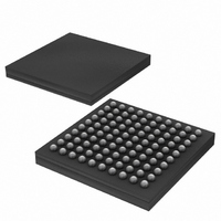
Manufacturer Part Number
DS3170N+
Description
IC TXRX DS3/E3 100-CSBGA
Manufacturer
Maxim Integrated Products
Datasheet
1.DS3170.pdf
(230 pages)
Specifications of DS3170N+
Function
Single-Chip Transceiver
Interface
DS3, E3
Number Of Circuits
1
Voltage - Supply
3.135 V ~ 3.465 V
Current - Supply
120mA
Operating Temperature
-40°C ~ 85°C
Mounting Type
Surface Mount
Package / Case
100-LBGA
Includes
DS3 Framers, E3 Framers, HDLC Controller, On-Chip BERTs
Lead Free Status / RoHS Status
Lead free / RoHS Compliant
Power (watts)
-


4 FEATURE DETAILS
The following sections describe the features provided by the DS3170 SCT.
4.1 Global Features
4.2 Receive DS3/E3 LIU Features
4.3 Jitter Attenuator Features
4.4 Receive DS3/E3 Framer Features
Supports the following transmission formats:
All controls and status fields are software accessible over either an 8/16-bit microprocessor port or a slave
serial bus communication port up to 10 Mbps (SPI)
On-chip clock rate adapter incorporates two separate internal PLLs to generate the necessary DS3 or E3 clock
used internally from an input clock reference (DS3, E3, 51.84 MHz, 77.76 MHz, or 19.44 MHz)
Optional transmit loop timed clock mode using the receive clock
Optional transmit clock mode using references generated by the internal Clock Rate Adapter (CLAD)
Clock, data and control signals can be inverted to allow a glueless interface to other devices
Detection of loss of transmit clock and loss of receive clock
Supports gapped 52 MHz clock rates for signals embedded in SONET/SDH
Jitter attenuator can be placed in either transmit or receive path when the LIU is enabled.
Automatic one-second, external or manual update of performance monitoring counters
Framing and line code error insertion available
Performs equalization, gain control, and clock and data recovery for incoming DS3 and E3 signals
AGC/Equalizer block handles from 0 dB to 15 dB of cable loss
Interfaces directly to a DSX-3 monitor signal (20 dB flat loss) using built-in pre-amp
Digital and analog Loss of Signal (LOS) detectors (ANSI T1.231 and ITU G.775)
Loss-of-lock status indication for internal phase-locked loop
Fully integrated, requires no external components
Standards-compliant jitter attenuation/jitter transfer
Can be inserted into the receive path or the transmit path
16-bit buffer depth
B3ZS/HDB3 decoding
Frame synchronization for M23 and C-bit Parity DS3, G.751 E3 and G.832 E3
Detection of RAI, AIS, DS3 idle signal, loss of signal (LOS), severely errored framing event (SEFE), change of
frame alignment (COFA), receipt of B3ZS/HDB3 codewords, DS3 application ID bit, DS3 M23/C-bit format
mismatch, G.751 national bit, and G.832 RDI (FERF), payload type, and timing marker bits
Detection and accumulation of bipolar violations (BPV), code violations (CV), excessive zeroes occurrences
(EXZ), F-bit errors, M-bit errors, FAS errors, LOF occurrences, P-bit parity errors, CP-bit parity errors, BIP-8
errors, and far end block errors (FEBE)
Manual or automatic one-second update of performance monitoring counters
The E3 national bit (Sn) is forwarded to a status register bit, the HDLC controller or the FEAC controller
HDLC controller with 256 byte FIFO for DS3 path maintenance data link (PMDL), G.751 national bit, or G.832
NR or GC channels
FEAC controller with four-codeword FIFO for DS3 FEAC channel
16-byte Trail Trace Buffer compares and stores G.832 trail access point identifier
DS3 M23 C-bits configurable as payload or overhead, stored in registers for software inspection
Most framing overhead fields presented on the receive overhead port
Framer pass-through mode for clear-channel applications and externally defined frame formats
C-Bit DS3
M23 DS3
G.751 E3
G.832 E3
13 of 230
DS3170 DS3/E3 Single-Chip Transceiver
Related parts for DS3170N+
Image
Part Number
Description
Manufacturer
Datasheet
Request
R

Part Number:
Description:
IC TXRX DS3/E3 100-CSBGA
Manufacturer:
Maxim Integrated Products
Datasheet:

Part Number:
Description:
Network Controller & Processor ICs DS3-E3 Single-Chip T ransceiver T3-E3 Fra
Manufacturer:
Maxim Integrated Products
Datasheet:
Part Number:
Description:
MAX7528KCWPMaxim Integrated Products [CMOS Dual 8-Bit Buffered Multiplying DACs]
Manufacturer:
Maxim Integrated Products
Datasheet:
Part Number:
Description:
Single +5V, fully integrated, 1.25Gbps laser diode driver.
Manufacturer:
Maxim Integrated Products
Datasheet:
Part Number:
Description:
Single +5V, fully integrated, 155Mbps laser diode driver.
Manufacturer:
Maxim Integrated Products
Datasheet:
Part Number:
Description:
VRD11/VRD10, K8 Rev F 2/3/4-Phase PWM Controllers with Integrated Dual MOSFET Drivers
Manufacturer:
Maxim Integrated Products
Datasheet:
Part Number:
Description:
Highly Integrated Level 2 SMBus Battery Chargers
Manufacturer:
Maxim Integrated Products
Datasheet:
Part Number:
Description:
Current Monitor and Accumulator with Integrated Sense Resistor; ; Temperature Range: -40°C to +85°C
Manufacturer:
Maxim Integrated Products
Part Number:
Description:
TSSOP 14/A°/RS-485 Transceivers with Integrated 100O/120O Termination Resis
Manufacturer:
Maxim Integrated Products
Part Number:
Description:
TSSOP 14/A°/RS-485 Transceivers with Integrated 100O/120O Termination Resis
Manufacturer:
Maxim Integrated Products
Part Number:
Description:
QFN 16/A°/AC-DC and DC-DC Peak-Current-Mode Converters with Integrated Step
Manufacturer:
Maxim Integrated Products
Part Number:
Description:
TDFN/A/65V, 1A, 600KHZ, SYNCHRONOUS STEP-DOWN REGULATOR WITH INTEGRATED SWI
Manufacturer:
Maxim Integrated Products
Part Number:
Description:
Integrated Temperature Controller f
Manufacturer:
Maxim Integrated Products
Part Number:
Description:
SOT23-6/I°/45MHz to 650MHz, Integrated IF VCOs with Differential Output
Manufacturer:
Maxim Integrated Products
Part Number:
Description:
SOT23-6/I°/45MHz to 650MHz, Integrated IF VCOs with Differential Output
Manufacturer:
Maxim Integrated Products