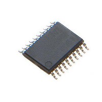
ATTINY861A-XU Atmel, ATTINY861A-XU Datasheet - Page 64

ATTINY861A-XU
Manufacturer Part Number
ATTINY861A-XU
Description
Microcontrollers (MCU) 8K Flash;125B EEPROM 128B SRAM;16 IO Pins
Manufacturer
Atmel
Datasheet
1.ATTINY861A-XU.pdf
(292 pages)
Specifications of ATTINY861A-XU
Core
RISC
Data Bus Width
8 bit
Program Memory Type
Flash
Program Memory Size
8 KB
Data Ram Size
512 B
Interface Type
SPI
Maximum Clock Frequency
20 MHz
Number Of Programmable I/os
16
Operating Supply Voltage
1.8 V to 5.5 V
Maximum Operating Temperature
+ 85 C
Mounting Style
SMD/SMT
Package / Case
TSSOP-20
Minimum Operating Temperature
- 40 C
Lead Free Status / Rohs Status
Details
Available stocks
Company
Part Number
Manufacturer
Quantity
Price
Company:
Part Number:
ATTINY861A-XUR
Manufacturer:
IDT
Quantity:
1 300
- Current page: 64 of 292
- Download datasheet (9Mb)
10.2.2
64
ATtiny261A/461A/861A
Alternate Functions of Port B
The Port B pins with alternate function are shown in
Table 10-6.
• Port B, Bit 7 - RESET/ dW/ ADC10/ PCINT15
• RESET, Reset pin: When the RSTDISBL Fuse is programmed, this pin functions as a normal
• If PB7 is used as a reset pin, DDB7, PORTB7 and PINB7 will all read 0.
• dW: When the debugWIRE Enable (DWEN) Fuse is programmed and Lock bits are
I/O pin, and the part will have to rely on Power-on Reset and Brown-out Reset as its reset
sources. When the RSTDISBL Fuse is unprogrammed, the reset circuitry is connected to the
pin, and the pin can not be used as an I/O pin.
unprogrammed, the RESET port pin is configured as a wire-AND (open-drain) bi-directional
I/O pin with pull-up enabled and becomes the communication gateway between target and
emulator.
Port Pin
PB7
PB6
PB5
PB4
PB3
PB2
PB1
PB0
Port B Pins Alternate Functions
Alternate Function
RESET: Reset pin
dW:
ADC10: ADC Input Channel 10
PCINT15:Pin Change Interrupt 0, Source 15
ADC9:
T0:
INT0:
PCINT14:Pin Change Interrupt 0, Source 14
XTAL2: Crystal Oscillator Output
CLKO: System Clock Output
OC1D: Timer/Counter1 Compare Match D Output
ADC8:
PCINT13:Pin Change Interrupt 0, Source 13
XTAL1: Crystal Oscillator Input
CLKI:
OC1D: Inverted Timer/Counter1 Compare Match D Output
ADC7:
PCINT12:Pin Change Interrupt 0, Source 12
OC1B: Timer/Counter1 Compare Match B Output
PCINT11:Pin Change Interrupt 0, Source 11
USCK: USI Clock (Three Wire Mode)
SCL :
OC1B: Inverted Timer/Counter1 Compare Match B Output
PCINT10:Pin Change Interrupt 0, Source 10
DO:
OC1A: Timer/Counter1 Compare Match A Output
PCINT9: Pin Change Interrupt 1, Source 9
DI:
SDA:
OC1A: Inverted Timer/Counter1 Compare Match A Output
PCINT8: Pin Change Interrupt 1, Source 8
debugWire I/O
ADC Input Channel 9
Timer/Counter0 Clock Source
External Interrupt 0 Input
ADC Input Channel 8
External Clock Input
ADC Input Channel 7
USI Clock (Two Wire Mode)
USI Data Output (Three Wire Mode)
USI Data Input (Three Wire Mode)
USI Data Input (Two Wire Mode)
Table
10-6.
8197B–AVR–01/10
Related parts for ATTINY861A-XU
Image
Part Number
Description
Manufacturer
Datasheet
Request
R

Part Number:
Description:
DEV KIT FOR AVR/AVR32
Manufacturer:
Atmel
Datasheet:

Part Number:
Description:
INTERVAL AND WIPE/WASH WIPER CONTROL IC WITH DELAY
Manufacturer:
ATMEL Corporation
Datasheet:

Part Number:
Description:
Low-Voltage Voice-Switched IC for Hands-Free Operation
Manufacturer:
ATMEL Corporation
Datasheet:

Part Number:
Description:
MONOLITHIC INTEGRATED FEATUREPHONE CIRCUIT
Manufacturer:
ATMEL Corporation
Datasheet:

Part Number:
Description:
AM-FM Receiver IC U4255BM-M
Manufacturer:
ATMEL Corporation
Datasheet:

Part Number:
Description:
Monolithic Integrated Feature Phone Circuit
Manufacturer:
ATMEL Corporation
Datasheet:

Part Number:
Description:
Multistandard Video-IF and Quasi Parallel Sound Processing
Manufacturer:
ATMEL Corporation
Datasheet:

Part Number:
Description:
High-performance EE PLD
Manufacturer:
ATMEL Corporation
Datasheet:

Part Number:
Description:
8-bit Flash Microcontroller
Manufacturer:
ATMEL Corporation
Datasheet:

Part Number:
Description:
2-Wire Serial EEPROM
Manufacturer:
ATMEL Corporation
Datasheet:


