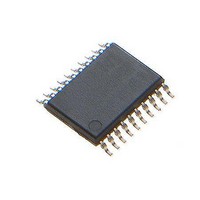
ATTINY861A-XU Atmel, ATTINY861A-XU Datasheet - Page 105

ATTINY861A-XU
Manufacturer Part Number
ATTINY861A-XU
Description
Microcontrollers (MCU) 8K Flash;125B EEPROM 128B SRAM;16 IO Pins
Manufacturer
Atmel
Datasheet
1.ATTINY861A-XU.pdf
(292 pages)
Specifications of ATTINY861A-XU
Core
RISC
Data Bus Width
8 bit
Program Memory Type
Flash
Program Memory Size
8 KB
Data Ram Size
512 B
Interface Type
SPI
Maximum Clock Frequency
20 MHz
Number Of Programmable I/os
16
Operating Supply Voltage
1.8 V to 5.5 V
Maximum Operating Temperature
+ 85 C
Mounting Style
SMD/SMT
Package / Case
TSSOP-20
Minimum Operating Temperature
- 40 C
Lead Free Status / Rohs Status
Details
Available stocks
Company
Part Number
Manufacturer
Quantity
Price
Company:
Part Number:
ATTINY861A-XUR
Manufacturer:
IDT
Quantity:
1 300
- Current page: 105 of 292
- Download datasheet (9Mb)
12.10 Fault Protection Unit
8197B–AVR–01/10
Figure 12-17. Timer/Counter Timing Diagram, Setting of OCF1x, with Prescaler (f
Figure 12-18
Figure 12-18. Timer/Counter Timing Diagram, with Prescaler (f
The Timer/Counter1 incorporates a Fault Protection unit, which can be set to disable the PWM
output pins when an external event is triggered. The external signal indicating an event can be
applied via the external interrupt INT0 pin or, alternatively, via the analog-comparator unit. The
Fault Protection unit is illustrated in
directly a part of the Fault Protection unit are gray shaded.
Figure 12-19. Fault Protection Unit Block Diagram
Fault Protection mode is enabled by setting the Fault Protection Enable (FPEN1) bit and trig-
gered by a change in logic level at external interrupt pin (INT0). Alternatively, fault protection
mode can be triggered by the Analog Comparator Output (ACO).
When Fault Protection is triggered, the COM1x bits are cleared, Output Comparators are discon-
nected from the PWM output pins and PORTB register bits are connected to the PWM output
TCNTn
(clk
TCNTn
OCRnx
(clk
OCFnx
TOVn
clk
clk
clk
INT0
clk
PCK
PCK
PCK
Tn
PCK
Tn
/8)
/8)
Comparator
shows the setting of TOV1 in Phase and Frequency Correct PWM Mode.
Analog
ACO*
BOTTOM + 1
OCRnx - 1
FPAC1
Figure
Canceler
FPNC1
Noise
BOTTOM + 1
12-19. The elements of the block diagram that are not
OCRnx
OCRnx Value
FPES1
Detector
Edge
FPEN1
OCRnx + 1
clkT1
BOTTOM
/8)
FAULT_PROTECTION (Int. Req.)
Timer/Counter1
BOTTOM + 1
clkT1
OCRnx + 2
/8)
105
Related parts for ATTINY861A-XU
Image
Part Number
Description
Manufacturer
Datasheet
Request
R

Part Number:
Description:
DEV KIT FOR AVR/AVR32
Manufacturer:
Atmel
Datasheet:

Part Number:
Description:
INTERVAL AND WIPE/WASH WIPER CONTROL IC WITH DELAY
Manufacturer:
ATMEL Corporation
Datasheet:

Part Number:
Description:
Low-Voltage Voice-Switched IC for Hands-Free Operation
Manufacturer:
ATMEL Corporation
Datasheet:

Part Number:
Description:
MONOLITHIC INTEGRATED FEATUREPHONE CIRCUIT
Manufacturer:
ATMEL Corporation
Datasheet:

Part Number:
Description:
AM-FM Receiver IC U4255BM-M
Manufacturer:
ATMEL Corporation
Datasheet:

Part Number:
Description:
Monolithic Integrated Feature Phone Circuit
Manufacturer:
ATMEL Corporation
Datasheet:

Part Number:
Description:
Multistandard Video-IF and Quasi Parallel Sound Processing
Manufacturer:
ATMEL Corporation
Datasheet:

Part Number:
Description:
High-performance EE PLD
Manufacturer:
ATMEL Corporation
Datasheet:

Part Number:
Description:
8-bit Flash Microcontroller
Manufacturer:
ATMEL Corporation
Datasheet:

Part Number:
Description:
2-Wire Serial EEPROM
Manufacturer:
ATMEL Corporation
Datasheet:


