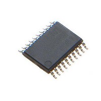
ATTINY861A-XU Atmel, ATTINY861A-XU Datasheet - Page 159

ATTINY861A-XU
Manufacturer Part Number
ATTINY861A-XU
Description
Microcontrollers (MCU) 8K Flash;125B EEPROM 128B SRAM;16 IO Pins
Manufacturer
Atmel
Datasheet
1.ATTINY861A-XU.pdf
(292 pages)
Specifications of ATTINY861A-XU
Core
RISC
Data Bus Width
8 bit
Program Memory Type
Flash
Program Memory Size
8 KB
Data Ram Size
512 B
Interface Type
SPI
Maximum Clock Frequency
20 MHz
Number Of Programmable I/os
16
Operating Supply Voltage
1.8 V to 5.5 V
Maximum Operating Temperature
+ 85 C
Mounting Style
SMD/SMT
Package / Case
TSSOP-20
Minimum Operating Temperature
- 40 C
Lead Free Status / Rohs Status
Details
Available stocks
Company
Part Number
Manufacturer
Quantity
Price
Company:
Part Number:
ATTINY861A-XUR
Manufacturer:
IDT
Quantity:
1 300
- Current page: 159 of 292
- Download datasheet (9Mb)
15.13.5
15.13.6
8197B–AVR–01/10
DIDR0 – Digital Input Disable Register 0
DIDR1 – Digital Input Disable Register 1
trigger signal. If ADEN in ADCSRA is set, this will start a conversion. Switching to Free Running
mode (ADTS[2:0]=0) will not cause a trigger event, even if the ADC Interrupt Flag is set
Table 15-6.
• Bits 7:4,2:0 – ADC6D:ADC0D: ADC6:0 Digital Input Disable
When this bit is written logic one, the digital input buffer on the corresponding ADC pin is dis-
abled. The corresponding PIN register bit will always read as zero when this bit is set. When an
analog signal is applied to the ADC7:0 pin and the digital input from this pin is not needed, this
bit should be written logic one to reduce power consumption in the digital input buffer.
• Bit 3 – AREFD: AREF Digital Input Disable
When this bit is written logic one, the digital input buffer on the AREF pin is disabled. The corre-
sponding PIN register bit will always read as zero when this bit is set. When an analog signal is
applied to the AREF pin and the digital input from this pin is not needed, this bit should be written
logic one to reduce power consumption in the digital input buffer.
• Bits 7:4 – ADC10D:ADC7D: ADC10:7 Digital Input Disable
When this bit is written logic one, the digital input buffer on the corresponding ADC pin is dis-
abled. The corresponding PIN register bit will always read as zero when this bit is set. When an
analog signal is applied to the ADC10:7 pin and the digital input from this pin is not needed, this
bit should be written logic one to reduce power consumption in the digital input buffer.
Bit
0x01 (0x21)
Read/Write
Initial Value
Bit
0x02 (0x22)
Read/Write
Initial Value
ADTS2
0
0
0
0
1
1
1
1
ADC Auto Trigger Source Selections
7
ADC6D
R/W
0
ADC10D
R/W
7
0
6
ADC5D
R/W
0
ADC9D
ADTS1
R/W
6
0
0
0
1
1
0
0
1
1
5
ADC4D
R/W
0
ADC8D
R/W
5
0
4
ADC3D
R/W
0
ADC7D
R/W
ADTS0
4
0
0
1
0
1
0
1
0
1
3
AREFD
R/W
0
R
3
0
-
Trigger Source
Free Running mode
Analog Comparator
External Interrupt Request 0
Timer/Counter0 Compare Match A
Timer/Counter0 Overflow
Timer/Counter0 Compare Match B
Timer/Counter1 Overflow
Watchdog Interrupt Request
2
ADC2D
R/W
0
R
2
0
1
ADC1D
R/W
0
R
1
0
0
ADC0D
R/W
0
R
0
0
DIDR0
.
DIDR1
159
Related parts for ATTINY861A-XU
Image
Part Number
Description
Manufacturer
Datasheet
Request
R

Part Number:
Description:
DEV KIT FOR AVR/AVR32
Manufacturer:
Atmel
Datasheet:

Part Number:
Description:
INTERVAL AND WIPE/WASH WIPER CONTROL IC WITH DELAY
Manufacturer:
ATMEL Corporation
Datasheet:

Part Number:
Description:
Low-Voltage Voice-Switched IC for Hands-Free Operation
Manufacturer:
ATMEL Corporation
Datasheet:

Part Number:
Description:
MONOLITHIC INTEGRATED FEATUREPHONE CIRCUIT
Manufacturer:
ATMEL Corporation
Datasheet:

Part Number:
Description:
AM-FM Receiver IC U4255BM-M
Manufacturer:
ATMEL Corporation
Datasheet:

Part Number:
Description:
Monolithic Integrated Feature Phone Circuit
Manufacturer:
ATMEL Corporation
Datasheet:

Part Number:
Description:
Multistandard Video-IF and Quasi Parallel Sound Processing
Manufacturer:
ATMEL Corporation
Datasheet:

Part Number:
Description:
High-performance EE PLD
Manufacturer:
ATMEL Corporation
Datasheet:

Part Number:
Description:
8-bit Flash Microcontroller
Manufacturer:
ATMEL Corporation
Datasheet:

Part Number:
Description:
2-Wire Serial EEPROM
Manufacturer:
ATMEL Corporation
Datasheet:


