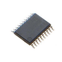
ATTINY861A-XU Atmel, ATTINY861A-XU Datasheet - Page 172

ATTINY861A-XU
Manufacturer Part Number
ATTINY861A-XU
Description
Microcontrollers (MCU) 8K Flash;125B EEPROM 128B SRAM;16 IO Pins
Manufacturer
Atmel
Datasheet
1.ATTINY861A-XU.pdf
(292 pages)
Specifications of ATTINY861A-XU
Core
RISC
Data Bus Width
8 bit
Program Memory Type
Flash
Program Memory Size
8 KB
Data Ram Size
512 B
Interface Type
SPI
Maximum Clock Frequency
20 MHz
Number Of Programmable I/os
16
Operating Supply Voltage
1.8 V to 5.5 V
Maximum Operating Temperature
+ 85 C
Mounting Style
SMD/SMT
Package / Case
TSSOP-20
Minimum Operating Temperature
- 40 C
Lead Free Status / Rohs Status
Details
Available stocks
Company
Part Number
Manufacturer
Quantity
Price
Company:
Part Number:
ATTINY861A-XUR
Manufacturer:
IDT
Quantity:
1 300
- Current page: 172 of 292
- Download datasheet (9Mb)
18.6.2
Table 18-11. Serial Programming Instruction Set
172
Instruction/Operation
Programming Enable
Chip Erase (Program Memory/EEPROM)
Poll RDY/BSY
Load Instructions
Load Extended Address byte
Load Program Memory Page, High byte
ATtiny261A/461A/861A
Serial Programming Instruction set
Table 18-10. Minimum Wait Delay Before Writing the Next Flash or EEPROM Location
The instruction set is described in
(1)
Symbol
t
t
t
t
5. A: The EEPROM array is programmed one byte at a time by supplying the address and
6. Any memory location can be verified by using the Read instruction which returns the
7. At the end of the programming session, RESET can be set high to commence normal
8. Power-off sequence (if needed):
WD_FLASH
WD_EEPROM
WD_ERASE
WD_FUSE
interface before the Flash write operation completes can result in incorrect
programming.
data together with the appropriate Write instruction. An EEPROM memory location is
first automatically erased before new data is written. If polling (RDY/BSY) is not used,
the user must wait at least t
In a chip erased device, no 0xFFs in the data file(s) need to be programmed.
B: The EEPROM array is programmed one page at a time. The Memory page is loaded
one byte at a time by supplying the 2 LSB of the address and data together with the
Load EEPROM Memory Page instruction. The EEPROM Memory Page is stored by
loading the Write EEPROM Memory Page Instruction with the 6 MSB of the address.
When using EEPROM page access only byte locations loaded with the Load EEPROM
Memory Page instruction is altered. The remaining locations remain unchanged. If poll-
ing (RDY/BSY) is not used, the used must wait at least t
next page (See
be programmed.
content at the selected address at serial output MISO.
operation.
Set RESET to “1”.
Turn V
CC
power off.
Table
Byte 1
$AC
$AC
$4D
$F0
$48
18-8). In a chip erased device, no 0xFF in the data file(s) need to
WD_EEPROM
Table 18-11
adr MSB
Byte 2
before issuing the next byte. (See
$53
$80
$00
$00
and
Instruction Format
Figure 18-2 on page
Minimum Wait Delay
Extended adr
WD_EEPROM
4.5 ms
4.0 ms
9.0 ms
4.5 ms
adr LSB
Byte 3
$00
$00
$00
174.
before issuing the
Table
high data byte in
data byte out
8197B–AVR–01/10
Byte4
$00
$00
$00
18-10.)
Related parts for ATTINY861A-XU
Image
Part Number
Description
Manufacturer
Datasheet
Request
R

Part Number:
Description:
DEV KIT FOR AVR/AVR32
Manufacturer:
Atmel
Datasheet:

Part Number:
Description:
INTERVAL AND WIPE/WASH WIPER CONTROL IC WITH DELAY
Manufacturer:
ATMEL Corporation
Datasheet:

Part Number:
Description:
Low-Voltage Voice-Switched IC for Hands-Free Operation
Manufacturer:
ATMEL Corporation
Datasheet:

Part Number:
Description:
MONOLITHIC INTEGRATED FEATUREPHONE CIRCUIT
Manufacturer:
ATMEL Corporation
Datasheet:

Part Number:
Description:
AM-FM Receiver IC U4255BM-M
Manufacturer:
ATMEL Corporation
Datasheet:

Part Number:
Description:
Monolithic Integrated Feature Phone Circuit
Manufacturer:
ATMEL Corporation
Datasheet:

Part Number:
Description:
Multistandard Video-IF and Quasi Parallel Sound Processing
Manufacturer:
ATMEL Corporation
Datasheet:

Part Number:
Description:
High-performance EE PLD
Manufacturer:
ATMEL Corporation
Datasheet:

Part Number:
Description:
8-bit Flash Microcontroller
Manufacturer:
ATMEL Corporation
Datasheet:

Part Number:
Description:
2-Wire Serial EEPROM
Manufacturer:
ATMEL Corporation
Datasheet:


