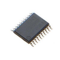
ATTINY861A-XU Atmel, ATTINY861A-XU Datasheet - Page 130

ATTINY861A-XU
Manufacturer Part Number
ATTINY861A-XU
Description
Microcontrollers (MCU) 8K Flash;125B EEPROM 128B SRAM;16 IO Pins
Manufacturer
Atmel
Datasheet
1.ATTINY861A-XU.pdf
(292 pages)
Specifications of ATTINY861A-XU
Core
RISC
Data Bus Width
8 bit
Program Memory Type
Flash
Program Memory Size
8 KB
Data Ram Size
512 B
Interface Type
SPI
Maximum Clock Frequency
20 MHz
Number Of Programmable I/os
16
Operating Supply Voltage
1.8 V to 5.5 V
Maximum Operating Temperature
+ 85 C
Mounting Style
SMD/SMT
Package / Case
TSSOP-20
Minimum Operating Temperature
- 40 C
Lead Free Status / Rohs Status
Details
Available stocks
Company
Part Number
Manufacturer
Quantity
Price
Company:
Part Number:
ATTINY861A-XUR
Manufacturer:
IDT
Quantity:
1 300
- Current page: 130 of 292
- Download datasheet (9Mb)
13.4.1
13.4.2
13.4.3
13.4.4
13.4.5
13.5
13.5.1
130
Register Descriptions
ATtiny261A/461A/861A
Half-Duplex Asynchronous Data Transfer
4-Bit Counter
12-Bit Timer/Counter
Edge Triggered External Interrupt
Software Interrupt
USIDR – USI Data Register
Using the USI Data Register in three-wire mode it is possible to implement a more compact and
higher performance UART than by software, only.
The 4-bit counter can be used as a stand-alone counter with overflow interrupt. Note that if the
counter is clocked externally, both clock edges will increment the counter value.
Combining the 4-bit USI counter with one of the 8-bit timer/counters creates a 12-bit counter.
By setting the counter to maximum value (F) it can function as an additional external interrupt.
The Overflow Flag and Interrupt Enable bit are then used for the external interrupt. This feature
is selected by the USICS1 bit.
The counter overflow interrupt can be used as a software interrupt triggered by a clock strobe.
The USI Data Register can be accessed directly.
Depending on the USICS1:0 bits of the USI Control Register a (left) shift operation may be per-
formed. The shift operation can be synchronised to an external clock edge, to a Timer/Counter0
Compare Match, or directly to software via the USICLK bit. If a serial clock occurs at the same
cycle the register is written, the register will contain the value written and no shift is performed.
Note that even when no wire mode is selected (USIWM1:0 = 0) both the external data input
(DI/SDA) and the external clock input (USCK/SCL) can still be used by the USI Data Register.
The output pin (DO or SDA, depending on the wire mode) is connected via the output latch to
the most significant bit (bit 7) of the USI Data Register. The output latch ensures that data input
is sampled and data output is changed on opposite clock edges. The latch is open (transparent)
during the first half of a serial clock cycle when an external clock source is selected (USICS1 =
1) and constantly open when an internal clock source is used (USICS1 = 0). The output will be
changed immediately when a new MSB is written as long as the latch is open.
Note that the Data Direction Register bit corresponding to the output pin must be set to one in
order to enable data output from the USI Data Register.
Bit
0x0F (0x2F)
Read/Write
Initial Value
7
MSB
R/W
0
6
R/W
0
5
R/W
0
4
R/W
0
3
R/W
0
2
0
R/W
1
R/W
0
0
LSB
R/W
0
8197B–AVR–01/10
USIDR
Related parts for ATTINY861A-XU
Image
Part Number
Description
Manufacturer
Datasheet
Request
R

Part Number:
Description:
DEV KIT FOR AVR/AVR32
Manufacturer:
Atmel
Datasheet:

Part Number:
Description:
INTERVAL AND WIPE/WASH WIPER CONTROL IC WITH DELAY
Manufacturer:
ATMEL Corporation
Datasheet:

Part Number:
Description:
Low-Voltage Voice-Switched IC for Hands-Free Operation
Manufacturer:
ATMEL Corporation
Datasheet:

Part Number:
Description:
MONOLITHIC INTEGRATED FEATUREPHONE CIRCUIT
Manufacturer:
ATMEL Corporation
Datasheet:

Part Number:
Description:
AM-FM Receiver IC U4255BM-M
Manufacturer:
ATMEL Corporation
Datasheet:

Part Number:
Description:
Monolithic Integrated Feature Phone Circuit
Manufacturer:
ATMEL Corporation
Datasheet:

Part Number:
Description:
Multistandard Video-IF and Quasi Parallel Sound Processing
Manufacturer:
ATMEL Corporation
Datasheet:

Part Number:
Description:
High-performance EE PLD
Manufacturer:
ATMEL Corporation
Datasheet:

Part Number:
Description:
8-bit Flash Microcontroller
Manufacturer:
ATMEL Corporation
Datasheet:

Part Number:
Description:
2-Wire Serial EEPROM
Manufacturer:
ATMEL Corporation
Datasheet:


