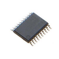
ATTINY861A-XU Atmel, ATTINY861A-XU Datasheet - Page 158

ATTINY861A-XU
Manufacturer Part Number
ATTINY861A-XU
Description
Microcontrollers (MCU) 8K Flash;125B EEPROM 128B SRAM;16 IO Pins
Manufacturer
Atmel
Datasheet
1.ATTINY861A-XU.pdf
(292 pages)
Specifications of ATTINY861A-XU
Core
RISC
Data Bus Width
8 bit
Program Memory Type
Flash
Program Memory Size
8 KB
Data Ram Size
512 B
Interface Type
SPI
Maximum Clock Frequency
20 MHz
Number Of Programmable I/os
16
Operating Supply Voltage
1.8 V to 5.5 V
Maximum Operating Temperature
+ 85 C
Mounting Style
SMD/SMT
Package / Case
TSSOP-20
Minimum Operating Temperature
- 40 C
Lead Free Status / Rohs Status
Details
Available stocks
Company
Part Number
Manufacturer
Quantity
Price
Company:
Part Number:
ATTINY861A-XUR
Manufacturer:
IDT
Quantity:
1 300
- Current page: 158 of 292
- Download datasheet (9Mb)
15.13.4
158
ATtiny261A/461A/861A
ADCSRB – ADC Control and Status Register B
If these bits are changed during a conversion, the change will not go into effect until this conver-
sion is complete (ADIF in ADCSRA is set).
• Bit 7– BIN: Bipolar Input Mode
The gain stage is working in the unipolar mode as default, but the bipolar mode can be selected
by writing the BIN bit in the ADCSRB register. In the unipolar mode only one-sided conversions
are supported and the voltage on the positive input must always be larger than the voltage on
the negative input. Otherwise the result is saturated to the voltage reference. In the bipolar mode
two-sided conversions are supported and the result is represented in the two’s complement
form. In the unipolar mode the resolution is 10 bits and the bipolar mode the resolution is 9 bits +
1 sign bit.
• Bits 6 – GSEL: Gain Select
The Gain Select bit selects the 32x gain instead of the 20x gain and the 8x gain instead of the 1x
gain when the Gain Select bit is written to one.
• Bits 5 – Res: Reserved Bit
This bit is reserved and will always read zero.
• Bits 4 – REFS2: Reference Selection Bit
These bit selects either the voltage reference of 1.1 V or 2.56 V for the ADC, as shown in
15-4. If active channels are used, using AVCC or an external AREF higher than (AVCC - 1V) is
not recommended, as this will affect ADC accuracy. The internal voltage reference options may
not be used if an external voltage is being applied to the AREF pin.
• Bits 3 – MUX5: Analog Channel and Gain Selection Bit 5
The MUX5 bit is the MSB of the Analog Channel and Gain Selection bits. Refer to
details. If this bit is changed during a conversion, the change will not go into effect until this
conversion is complete (ADIF in ADCSRA is set).
• Bits 2:0 – ADTS2:0: ADC Auto Trigger Source
If ADATE in ADCSRA is written to one, the value of these bits selects which source will trigger
an ADC conversion. If ADATE is cleared, the ADTS2:0 settings will have no effect. A conversion
will be triggered by the rising edge of the selected Interrupt Flag. Note that switching from a trig-
ger source that is cleared to a trigger source that is set, will generate a positive edge on the
Bit
0x03 (0x23)
Read/Write
Initial Value
R/W
BIN
7
0
GSEL
R/W
6
0
R
5
0
-
REFS2
R/W
4
0
MUX5
R/W
3
0
ADTS2
R/W
2
0
ADTS1
R/W
1
0
ADTS0
R/W
0
0
Table 15-5
8197B–AVR–01/10
ADCSRB
Table
for
Related parts for ATTINY861A-XU
Image
Part Number
Description
Manufacturer
Datasheet
Request
R

Part Number:
Description:
DEV KIT FOR AVR/AVR32
Manufacturer:
Atmel
Datasheet:

Part Number:
Description:
INTERVAL AND WIPE/WASH WIPER CONTROL IC WITH DELAY
Manufacturer:
ATMEL Corporation
Datasheet:

Part Number:
Description:
Low-Voltage Voice-Switched IC for Hands-Free Operation
Manufacturer:
ATMEL Corporation
Datasheet:

Part Number:
Description:
MONOLITHIC INTEGRATED FEATUREPHONE CIRCUIT
Manufacturer:
ATMEL Corporation
Datasheet:

Part Number:
Description:
AM-FM Receiver IC U4255BM-M
Manufacturer:
ATMEL Corporation
Datasheet:

Part Number:
Description:
Monolithic Integrated Feature Phone Circuit
Manufacturer:
ATMEL Corporation
Datasheet:

Part Number:
Description:
Multistandard Video-IF and Quasi Parallel Sound Processing
Manufacturer:
ATMEL Corporation
Datasheet:

Part Number:
Description:
High-performance EE PLD
Manufacturer:
ATMEL Corporation
Datasheet:

Part Number:
Description:
8-bit Flash Microcontroller
Manufacturer:
ATMEL Corporation
Datasheet:

Part Number:
Description:
2-Wire Serial EEPROM
Manufacturer:
ATMEL Corporation
Datasheet:


