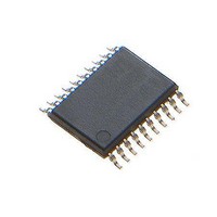
ATTINY861A-XU Atmel, ATTINY861A-XU Datasheet - Page 113

ATTINY861A-XU
Manufacturer Part Number
ATTINY861A-XU
Description
Microcontrollers (MCU) 8K Flash;125B EEPROM 128B SRAM;16 IO Pins
Manufacturer
Atmel
Datasheet
1.ATTINY861A-XU.pdf
(292 pages)
Specifications of ATTINY861A-XU
Core
RISC
Data Bus Width
8 bit
Program Memory Type
Flash
Program Memory Size
8 KB
Data Ram Size
512 B
Interface Type
SPI
Maximum Clock Frequency
20 MHz
Number Of Programmable I/os
16
Operating Supply Voltage
1.8 V to 5.5 V
Maximum Operating Temperature
+ 85 C
Mounting Style
SMD/SMT
Package / Case
TSSOP-20
Minimum Operating Temperature
- 40 C
Lead Free Status / Rohs Status
Details
Available stocks
Company
Part Number
Manufacturer
Quantity
Price
Company:
Part Number:
ATTINY861A-XUR
Manufacturer:
IDT
Quantity:
1 300
- Current page: 113 of 292
- Download datasheet (9Mb)
12.12.2
8197B–AVR–01/10
TCCR1B – Timer/Counter1 Control Register B
COM1B1S and COM1B0S in TCCR1C will show here. See
Register C” on page
• Bit 3 - FOC1A: Force Output Compare Match 1A
The FOC1A bit is only active when the PWM1A bit specify a non-PWM mode.
Writing a logical one to this bit forces a change in the Waveform Output (OCW1A) and the Out-
put Compare pin (OC1A) according to the values already set in COM1A1 and COM1A0. If
COM1A1 and COM1A0 written in the same cycle as FOC1A, the new settings will be used. The
Force Output Compare bit can be used to change the output pin value regardless of the timer
value. The automatic action programmed in COM1A1 and COM1A0 takes place as if a compare
match had occurred, but no interrupt is generated.
The FOC1A bit always reads zero.
• Bit 2 - FOC1B: Force Output Compare Match 1B
The FOC1B bit is only active when the PWM1B bit specify a non-PWM mode.
Writing a logical one to this bit forces a change in the Waveform Output (OCW1B) and the Out-
put Compare pin (OC1B) according to the values already set in COM1B1 and COM1B0. If
COM1B1 and COM1B0 written in the same cycle as FOC1B, the new settings will be used. The
Force Output Compare bit can be used to change the output pin value regardless of the timer
value. The automatic action programmed in COM1B1 and COM1B0 takes place as if a compare
match had occurred, but no interrupt is generated.
The FOC1B bit always reads zero.
• Bit 1 - PWM1A: Pulse Width Modulator A Enable
When set (one) this bit enables PWM mode based on comparator OCR1A
• Bit 0 - PWM1B: Pulse Width Modulator B Enable
When set (one) this bit enables PWM mode based on comparator OCR1B.
• Bit 7 - PWM1X : PWM Inversion Mode
When this bit is set (one), the PWM Inversion Mode is selected and the Dead Time Generator
outputs, OC1x and OC1x are inverted.
• Bit 6 - PSR1 : Prescaler Reset Timer/Counter1
When this bit is set (one), the Timer/Counter1 prescaler (TCNT1 is unaffected) will be reset. The
bit will be cleared by hardware after the operation is performed. Writing a zero to this bit will have
no effect. This bit will always read as zero.
• Bits 5,4 - DTPS11, DTPS10: Dead Time Prescaler Bits
The Timer/Counter1 Control Register B is a 8-bit read/write register.
Bit
0x2F (0x4F)
Read/Write
Initial value
PWM1X
R/W
7
0
115.
PSR1
R/W
6
0
DTPS11
R/W
5
0
DTPS10
R/W
4
0
CS13
R/W
3
0
“TCCR1C – Timer/Counter1 Control
CS12
R/W
2
0
CS11
R/W
1
0
CS10
R/W
0
0
TCCR1B
113
Related parts for ATTINY861A-XU
Image
Part Number
Description
Manufacturer
Datasheet
Request
R

Part Number:
Description:
DEV KIT FOR AVR/AVR32
Manufacturer:
Atmel
Datasheet:

Part Number:
Description:
INTERVAL AND WIPE/WASH WIPER CONTROL IC WITH DELAY
Manufacturer:
ATMEL Corporation
Datasheet:

Part Number:
Description:
Low-Voltage Voice-Switched IC for Hands-Free Operation
Manufacturer:
ATMEL Corporation
Datasheet:

Part Number:
Description:
MONOLITHIC INTEGRATED FEATUREPHONE CIRCUIT
Manufacturer:
ATMEL Corporation
Datasheet:

Part Number:
Description:
AM-FM Receiver IC U4255BM-M
Manufacturer:
ATMEL Corporation
Datasheet:

Part Number:
Description:
Monolithic Integrated Feature Phone Circuit
Manufacturer:
ATMEL Corporation
Datasheet:

Part Number:
Description:
Multistandard Video-IF and Quasi Parallel Sound Processing
Manufacturer:
ATMEL Corporation
Datasheet:

Part Number:
Description:
High-performance EE PLD
Manufacturer:
ATMEL Corporation
Datasheet:

Part Number:
Description:
8-bit Flash Microcontroller
Manufacturer:
ATMEL Corporation
Datasheet:

Part Number:
Description:
2-Wire Serial EEPROM
Manufacturer:
ATMEL Corporation
Datasheet:


