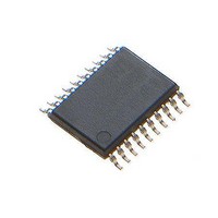
ATTINY861A-XU Atmel, ATTINY861A-XU Datasheet - Page 166

ATTINY861A-XU
Manufacturer Part Number
ATTINY861A-XU
Description
Microcontrollers (MCU) 8K Flash;125B EEPROM 128B SRAM;16 IO Pins
Manufacturer
Atmel
Datasheet
1.ATTINY861A-XU.pdf
(292 pages)
Specifications of ATTINY861A-XU
Core
RISC
Data Bus Width
8 bit
Program Memory Type
Flash
Program Memory Size
8 KB
Data Ram Size
512 B
Interface Type
SPI
Maximum Clock Frequency
20 MHz
Number Of Programmable I/os
16
Operating Supply Voltage
1.8 V to 5.5 V
Maximum Operating Temperature
+ 85 C
Mounting Style
SMD/SMT
Package / Case
TSSOP-20
Minimum Operating Temperature
- 40 C
Lead Free Status / Rohs Status
Details
Available stocks
Company
Part Number
Manufacturer
Quantity
Price
Company:
Part Number:
ATTINY861A-XUR
Manufacturer:
IDT
Quantity:
1 300
- Current page: 166 of 292
- Download datasheet (9Mb)
17.9
17.9.1
166
Register Description
ATtiny261A/461A/861A
SPMCSR – Store Program Memory Control and Status Register
The Store Program Memory Control and Status Register contains the control bits needed to con-
trol the Program memory operations.
• Bits 7:5 – Res: Reserved Bits
These bits are reserved and always read as zero.
• Bit 4 – CTPB: Clear Temporary Page Buffer
If the CTPB bit is written while filling the temporary page buffer, the temporary page buffer will be
cleared and the data will be lost.
• Bit 3 – RFLB: Read Fuse and Lock Bits
An LPM instruction within three cycles after RFLB and SPMEN are set in the SPMCSR Register,
will read either the Lock bits or the Fuse bits (depending on Z0 in the Z-pointer) into the destina-
tion register. See
• Bit 2 – PGWRT: Page Write
If this bit is written to one at the same time as SPMEN, the next SPM instruction within four clock
cycles executes Page Write, with the data stored in the temporary buffer. The page address is
taken from the high part of the Z-pointer. The data in R1 and R0 are ignored. The PGWRT bit
will auto-clear upon completion of a Page Write, or if no SPM instruction is executed within four
clock cycles. The CPU is halted during the entire Page Write operation.
• Bit 1 – PGERS: Page Erase
If this bit is written to one at the same time as SPMEN, the next SPM instruction within four clock
cycles executes Page Erase. The page address is taken from the high part of the Z-pointer. The
data in R1 and R0 are ignored. The PGERS bit will auto-clear upon completion of a Page Erase,
or if no SPM instruction is executed within four clock cycles. The CPU is halted during the entire
Page Write operation.
• Bit 0 – SPMEN: Store Program Memory Enable
This bit enables the SPM instruction for the next four clock cycles. If written to one together with
either CTPB, RFLB, PGWRT, or PGERS, the following SPM instruction will have a special
meaning, see description above. If only SPMEN is written, the following SPM instruction will
store the value in R1:R0 in the temporary page buffer addressed by the Z-pointer. The LSB of
the Z-pointer is ignored. The SPMEN bit will auto-clear upon completion of an SPM instruction,
or if no SPM instruction is executed within four clock cycles. During Page Erase and Page Write,
the SPMEN bit remains high until the operation is completed.
Writing any other combination than “10001”, “01001”, “00101”, “00011” or “00001” in the lower
five bits will have no effect.
Bit
0x37 (0x57)
Read/Write
Initial Value
7
–
R
0
“EEPROM Write Prevents Writing to SPMCSR” on page 164
6
–
R
0
5
–
R
0
4
CTPB
R/W
0
3
RFLB
R/W
0
2
PGWRT
R/W
0
1
PGERS
R/W
0
0
SPMEN
R/W
0
for details.
8197B–AVR–01/10
SPMCSR
Related parts for ATTINY861A-XU
Image
Part Number
Description
Manufacturer
Datasheet
Request
R

Part Number:
Description:
DEV KIT FOR AVR/AVR32
Manufacturer:
Atmel
Datasheet:

Part Number:
Description:
INTERVAL AND WIPE/WASH WIPER CONTROL IC WITH DELAY
Manufacturer:
ATMEL Corporation
Datasheet:

Part Number:
Description:
Low-Voltage Voice-Switched IC for Hands-Free Operation
Manufacturer:
ATMEL Corporation
Datasheet:

Part Number:
Description:
MONOLITHIC INTEGRATED FEATUREPHONE CIRCUIT
Manufacturer:
ATMEL Corporation
Datasheet:

Part Number:
Description:
AM-FM Receiver IC U4255BM-M
Manufacturer:
ATMEL Corporation
Datasheet:

Part Number:
Description:
Monolithic Integrated Feature Phone Circuit
Manufacturer:
ATMEL Corporation
Datasheet:

Part Number:
Description:
Multistandard Video-IF and Quasi Parallel Sound Processing
Manufacturer:
ATMEL Corporation
Datasheet:

Part Number:
Description:
High-performance EE PLD
Manufacturer:
ATMEL Corporation
Datasheet:

Part Number:
Description:
8-bit Flash Microcontroller
Manufacturer:
ATMEL Corporation
Datasheet:

Part Number:
Description:
2-Wire Serial EEPROM
Manufacturer:
ATMEL Corporation
Datasheet:


