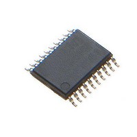
ATTINY861A-XU Atmel, ATTINY861A-XU Datasheet - Page 61

ATTINY861A-XU
Manufacturer Part Number
ATTINY861A-XU
Description
Microcontrollers (MCU) 8K Flash;125B EEPROM 128B SRAM;16 IO Pins
Manufacturer
Atmel
Datasheet
1.ATTINY861A-XU.pdf
(292 pages)
Specifications of ATTINY861A-XU
Core
RISC
Data Bus Width
8 bit
Program Memory Type
Flash
Program Memory Size
8 KB
Data Ram Size
512 B
Interface Type
SPI
Maximum Clock Frequency
20 MHz
Number Of Programmable I/os
16
Operating Supply Voltage
1.8 V to 5.5 V
Maximum Operating Temperature
+ 85 C
Mounting Style
SMD/SMT
Package / Case
TSSOP-20
Minimum Operating Temperature
- 40 C
Lead Free Status / Rohs Status
Details
Available stocks
Company
Part Number
Manufacturer
Quantity
Price
Company:
Part Number:
ATTINY861A-XUR
Manufacturer:
IDT
Quantity:
1 300
- Current page: 61 of 292
- Download datasheet (9Mb)
10.2.1
8197B–AVR–01/10
Alternate Functions of Port A
The Port A pins with alternate function are shown in
Table 10-3.
• Port A, Bit 7- ADC6/AIN0/PCINT7
• Port A, Bit 6 - ADC5/AIN1/PCINT6
• ADC6: Analog to Digital Converter, Channel 6
• AIN0: Analog Comparator Input. Configure the port pin as input with the internal pull-up
• PCINT7: Pin Change Interrupt source 8.
• ADC5: Analog to Digital Converter, Channel 5.
• AIN1: Analog Comparator Input. Configure the port pin as input with the internal pull-up
• PCINT6: Pin Change Interrupt source 6.
switched off to avoid the digital port function from interfering with the function of the Analog
Comparator.
switched off to avoid the digital port function from interfering with the function of the Analog
Comparator.
Port Pin
PA7
PA6
PA5
PA4
PA3
PA2
PA1
PA0
Port B Pins Alternate Functions
Alternate Function
ADC6:
AIN0:
PCINT7: Pin Change Interrupt 0, Source 7
ADC5:
AIN1:
PCINT6: Pin Change Interrupt 0, Source 6
ADC4:
AIN2:
PCINT5: Pin Change Interrupt 0, Source 5
ADC3:
ICP0:
PCINT4: Pin Change Interrupt 0, Source 4
AREF:
PCINT3: Pin Change Interrupt 0, Source 3
ADC2:
INT1:
USCK: USI Clock (Three Wire Mode)
SCL :
PCINT2: Pin Change Interrupt 0, Source 2
ADC1:
DO:
PCINT1:Pin Change Interrupt 0, Source 1
ADC0:
DI:
SDA:
PCINT0: Pin Change Interrupt 0, Source 0
ADC Input Channel 6
Analog Comparator Input
ADC Input Channel 5
Analog Comparator Input
ADC Input Channel 4
Analog Comparator Input
ADC Input Channel 3
Timer/Counter0 Input Capture Pin
External Analog Reference
ADC Input Channel 2
External Interrupt 1 Input
USI Clock (Two Wire Mode)
ADC Input Channel 1
USI Data Output (Three Wire Mode)
ADC Input Channel 0
USI Data Input (Three Wire Mode)
USI Data Input (Two Wire Mode)
.
Table
10-3.
61
Related parts for ATTINY861A-XU
Image
Part Number
Description
Manufacturer
Datasheet
Request
R

Part Number:
Description:
DEV KIT FOR AVR/AVR32
Manufacturer:
Atmel
Datasheet:

Part Number:
Description:
INTERVAL AND WIPE/WASH WIPER CONTROL IC WITH DELAY
Manufacturer:
ATMEL Corporation
Datasheet:

Part Number:
Description:
Low-Voltage Voice-Switched IC for Hands-Free Operation
Manufacturer:
ATMEL Corporation
Datasheet:

Part Number:
Description:
MONOLITHIC INTEGRATED FEATUREPHONE CIRCUIT
Manufacturer:
ATMEL Corporation
Datasheet:

Part Number:
Description:
AM-FM Receiver IC U4255BM-M
Manufacturer:
ATMEL Corporation
Datasheet:

Part Number:
Description:
Monolithic Integrated Feature Phone Circuit
Manufacturer:
ATMEL Corporation
Datasheet:

Part Number:
Description:
Multistandard Video-IF and Quasi Parallel Sound Processing
Manufacturer:
ATMEL Corporation
Datasheet:

Part Number:
Description:
High-performance EE PLD
Manufacturer:
ATMEL Corporation
Datasheet:

Part Number:
Description:
8-bit Flash Microcontroller
Manufacturer:
ATMEL Corporation
Datasheet:

Part Number:
Description:
2-Wire Serial EEPROM
Manufacturer:
ATMEL Corporation
Datasheet:


