PSMN1R5-40ES,127 NXP Semiconductors, PSMN1R5-40ES,127 Datasheet - Page 2
PSMN1R5-40ES,127
Manufacturer Part Number
PSMN1R5-40ES,127
Description
MOSFET Power N-Ch 40V 1.6 mOhms
Manufacturer
NXP Semiconductors
Series
-r
Datasheet
1.PSMN1R5-40ES127.pdf
(14 pages)
Specifications of PSMN1R5-40ES,127
Transistor Polarity
N-Channel
Resistance Drain-source Rds (on)
1.6 mOhms
Drain-source Breakdown Voltage
40 V
Gate-source Breakdown Voltage
20 V
Continuous Drain Current
120 A
Power Dissipation
338 W
Maximum Operating Temperature
+ 175 C
Mounting Style
SMD/SMT
Package / Case
I2PAK
Gate Charge Qg
133 nC
Minimum Operating Temperature
- 55 C
Fet Type
MOSFET N-Channel, Metal Oxide
Fet Feature
Standard
Rds On (max) @ Id, Vgs
1.6 mOhm @ 25A, 10V
Drain To Source Voltage (vdss)
40V
Current - Continuous Drain (id) @ 25° C
120A
Vgs(th) (max) @ Id
4V @ 1mA
Gate Charge (qg) @ Vgs
136nC @ 10V
Input Capacitance (ciss) @ Vds
9710pF @ 20V
Power - Max
338W
Mounting Type
Through Hole
Lead Free Status / Rohs Status
Details
Other names
934065161127


NXP Semiconductors
2. Pinning information
Table 2.
3. Ordering information
Table 3.
4. Limiting values
Table 4.
In accordance with the Absolute Maximum Rating System (IEC 60134).
[1]
PSMN1R5-40ES
Product data sheet
Pin
1
2
3
mb
Type number
PSMN1R5-40ES
Symbol
V
V
V
I
I
P
T
T
T
Source-drain diode
I
I
Avalanche ruggedness
E
D
DM
S
SM
stg
j
sld(M)
DS
DGR
GS
tot
DS(AL)S
Continuous current is limited by package.
Symbol Description
G
D
S
D
Pinning information
Ordering information
Limiting values
Parameter
drain-source voltage
drain-gate voltage
gate-source voltage
drain current
peak drain current
total power dissipation
storage temperature
junction temperature
peak soldering temperature
source current
peak source current
non-repetitive drain-source
avalanche energy
gate
drain
source
drain
Package
Name
I2PAK
Description
plastic single-ended package (I2PAK); TO-262
All information provided in this document is subject to legal disclaimers.
Conditions
T
T
V
V
pulsed; t
T
T
pulsed; t
V
V
t
p
j
j
mb
mb
GS
GS
GS
sup
= 0.1 ms
Rev. 01 — 19 April 2011
≥ 25 °C; T
≥ 25 °C; T
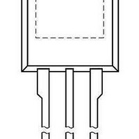
Simplified outline
= 25 °C; see
= 25 °C
= 10 V; T
= 10 V; T
= 10 V; T
≤ 40 V; unclamped; R
N-channel 40 V 1.6 mΩ standard level MOSFET in I2PAK.
p
p
SOT226 (I2PAK)
≤ 10 µs; T
≤ 10 µs; T
j
j
≤ 175 °C
≤ 175 °C; R
mb
mb
j(init)
1
= 100 °C
= 25 °C; see
mb
Figure 2
2
= 25 °C; I
mb
mb
3
= 25 °C; see
= 25 °C
GS
GS
D
= 20 kΩ
= 120 A;
= 50 Ω;
Figure 1
Graphic symbol
Figure 3
PSMN1R5-40ES
[1]
[1]
[1]
mbb076
G
Min
-
-
-20
-
-
-
-
-55
-55
-
-
-
-
© NXP B.V. 2011. All rights reserved.
D
S
SOT226
175
175
260
Version
Max
40
40
20
120
120
1301
338
120
1301
1.4
Unit
V
V
V
A
A
A
W
°C
°C
°C
A
A
J
2 of 14
Related parts for PSMN1R5-40ES,127
Image
Part Number
Description
Manufacturer
Datasheet
Request
R

Part Number:
Description:
MOSFET Power N-Ch 40V 1.6 mOhms
Manufacturer:
NXP Semiconductors
Datasheet:

Part Number:
Description:
MOSFET N-CH 25V 100A LFPAK
Manufacturer:
NXP Semiconductors
Datasheet:

Part Number:
Description:
MOSFET,N CH,30V,100A,LFPAK
Manufacturer:
NXP Semiconductors
Datasheet:

Part Number:
Description:
MOSFET Power N-Ch 30V 1.55mOhms
Manufacturer:
NXP Semiconductors
Datasheet:

Part Number:
Description:
Logic level N-channel enhancement mode Field-Effect Transistor (FET) in a plastic package using TrenchMOS technology
Manufacturer:
NXP Semiconductors
Datasheet:
Part Number:
Description:
Logic level enhancement mode N-channel MOSFET in LFPAK package
Manufacturer:
NXP Semiconductors
Datasheet:

Part Number:
Description:
Standard level N-channel MOSFET in I2PAK (SOT226) package qualified to 175 �C
Manufacturer:
NXP Semiconductors
Datasheet:

Part Number:
Description:
Standard level N-channel MOSFET in TO220 (SOT78) package qualified to 175 �C
Manufacturer:
NXP Semiconductors
Datasheet:
Part Number:
Description:
MOSFET N-CH 30V LFPAK
Manufacturer:
NXP Semiconductors
Datasheet:

Part Number:
Description:
NXP Semiconductors designed the LPC2420/2460 microcontroller around a 16-bit/32-bitARM7TDMI-S CPU core with real-time debug interfaces that include both JTAG andembedded trace
Manufacturer:
NXP Semiconductors
Datasheet:

Part Number:
Description:
NXP Semiconductors designed the LPC2458 microcontroller around a 16-bit/32-bitARM7TDMI-S CPU core with real-time debug interfaces that include both JTAG andembedded trace
Manufacturer:
NXP Semiconductors
Datasheet:
Part Number:
Description:
NXP Semiconductors designed the LPC2468 microcontroller around a 16-bit/32-bitARM7TDMI-S CPU core with real-time debug interfaces that include both JTAG andembedded trace
Manufacturer:
NXP Semiconductors
Datasheet:
Part Number:
Description:
NXP Semiconductors designed the LPC2470 microcontroller, powered by theARM7TDMI-S core, to be a highly integrated microcontroller for a wide range ofapplications that require advanced communications and high quality graphic displays
Manufacturer:
NXP Semiconductors
Datasheet:
Part Number:
Description:
NXP Semiconductors designed the LPC2478 microcontroller, powered by theARM7TDMI-S core, to be a highly integrated microcontroller for a wide range ofapplications that require advanced communications and high quality graphic displays
Manufacturer:
NXP Semiconductors
Datasheet:
Part Number:
Description:
The Philips Semiconductors XA (eXtended Architecture) family of 16-bit single-chip microcontrollers is powerful enough to easily handle the requirements of high performance embedded applications, yet inexpensive enough to compete in the market for hi
Manufacturer:
NXP Semiconductors
Datasheet: