PSMN1R5-40ES,127 NXP Semiconductors, PSMN1R5-40ES,127 Datasheet
PSMN1R5-40ES,127
Specifications of PSMN1R5-40ES,127


Related parts for PSMN1R5-40ES,127


PSMN1R5-40ES,127 Summary of contents
Page 1
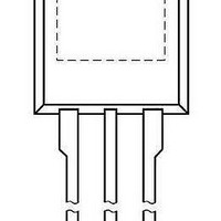
... PSMN1R5-40ES N-channel 40 V 1.6 mΩ standard level MOSFET in I2PAK. Rev. 01 — 19 April 2011 1. Product profile 1.1 General description Standard level N-channel MOSFET in I2PAK (SOT226) package qualified to 175 °C. This product is designed and qualified for use in a wide range of industrial, communications and domestic equipment. ...
Page 2
... °C; see Figure °C mb ≤ 10 µs; T pulsed ° ° j(init) ≤ unclamped sup All information provided in this document is subject to legal disclaimers. Rev. 01 — 19 April 2011 PSMN1R5-40ES Graphic symbol mbb076 SOT226 Min - = 20 kΩ - -20 [1] - [1] Figure 1 - Figure -55 175 -55 175 - 260 [ 120 A ...
Page 3
... Product data sheet N-channel 40 V 1.6 mΩ standard level MOSFET in I2PAK. 003a a f329 150 200 T (°C) mb Fig All information provided in this document is subject to legal disclaimers. Rev. 01 — 19 April 2011 PSMN1R5-40ES 120 P der (%) 100 Normalized total power dissipation as a function of mounting base temperature ...
Page 4
... Transient thermal impedance from junction to mounting base as a function of pulse duration PSMN1R5-40ES Product data sheet N-channel 40 V 1.6 mΩ standard level MOSFET in I2PAK. Conditions see Figure 4 Vertical in free air - All information provided in this document is subject to legal disclaimers. Rev. 01 — 19 April 2011 PSMN1R5-40ES Min Typ Max - 0.22 0. 003aaf327 tp δ ...
Page 5
... Figure 14; see Figure see Figure 14; DS see Figure MHz °C; see Figure 0.8 Ω 4.7 Ω R G(ext) All information provided in this document is subject to legal disclaimers. Rev. 01 — 19 April 2011 PSMN1R5-40ES Min Typ Max = -55 ° ° 4 ° 175 °C - 250 500 = 25 ° ...
Page 6
... GS DS 003aaf316 ( (A) D Fig 6. Transfer characteristics: drain current as a function of gate-source voltage; typical values All information provided in this document is subject to legal disclaimers. Rev. 01 — 19 April 2011 PSMN1R5-40ES Min Typ = 25 ° 117 = 25 °C j 003aaf317 = 175 ° ° © NXP B.V. 2011. All rights reserved. ...
Page 7
... V GS(th) (V) C iss C rss (V) GS Fig 10. Gate-source threshold voltage as a function of All information provided in this document is subject to legal disclaimers. Rev. 01 — 19 April 2011 PSMN1R5-40ES 20 6.0 5.0 5 0.25 0.5 0.75 Output characteristics: drain current as a function of drain-source voltage; typical values 5 4 max ...
Page 8
... V (V) GS Fig 12. Normalized drain-source on state resistance 003aaf326 4 (A) D Fig 14. Gate charge waveform definitions All information provided in this document is subject to legal disclaimers. Rev. 01 — 19 April 2011 PSMN1R5-40ES 2 1.5 1 0 120 factor as a function of junction temperature GS(pl) V GS(th ...
Page 9
... Fig 16. Input, output and reverse transfer capacitances ( 175 ° 0.25 0.5 0.75 All information provided in this document is subject to legal disclaimers. Rev. 01 — 19 April 2011 PSMN1R5-40ES - function of drain-source voltage; typical values 003aaf325 = 25 ° (V) SD © NXP B.V. 2011. All rights reserved. 003aaf324 C ...
Page 10
... max 0.7 1.6 10.3 11 2.54 0.4 1.2 9.7 REFERENCES JEDEC JEITA TO-262 All information provided in this document is subject to legal disclaimers. Rev. 01 — 19 April 2011 PSMN1R5-40ES mounting base 15.0 3.30 2.6 13.5 2.79 2.2 EUROPEAN PROJECTION SOT226 ISSUE DATE 06-02-14 09-08-25 © ...
Page 11
... NXP Semiconductors 8. Revision history Table 7. Revision history Document ID Release date PSMN1R5-40ES v.1 20110419 PSMN1R5-40ES Product data sheet N-channel 40 V 1.6 mΩ standard level MOSFET in I2PAK. Data sheet status Change notice Product data sheet - All information provided in this document is subject to legal disclaimers. ...
Page 12
... Characteristics sections of this document is not warranted. Constant or repeated exposure to limiting values will permanently and irreversibly affect the quality and reliability of the device. All information provided in this document is subject to legal disclaimers. Rev. 01 — 19 April 2011 PSMN1R5-40ES © NXP B.V. 2011. All rights reserved ...
Page 13
... TrenchMOS, TriMedia and UCODE — are trademarks of NXP B.V. HD Radio and HD Radio logo — are trademarks of iBiquity Digital Corporation. http://www.nxp.com salesaddresses@nxp.com All information provided in this document is subject to legal disclaimers. Rev. 01 — 19 April 2011 PSMN1R5-40ES Trademarks © NXP B.V. 2011. All rights reserved ...
Page 14
... Please be aware that important notices concerning this document and the product(s) described herein, have been included in section ‘Legal information’. © NXP B.V. 2011. For more information, please visit: http://www.nxp.com For sales office addresses, please send an email to: salesaddresses@nxp.com All rights reserved. Date of release: 19 April 2011 Document identifier: PSMN1R5-40ES ...