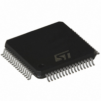
STLC5048TR STMicroelectronics, STLC5048TR Datasheet - Page 18

STLC5048TR
Manufacturer Part Number
STLC5048TR
Description
IC CODEC/FILTER PROGR 4CH 64TQFP
Manufacturer
STMicroelectronics
Type
PCM Codec/Filterr
Specifications of STLC5048TR
Data Interface
PCM Audio Interface
Resolution (bits)
16 b
Number Of Adcs / Dacs
4 / 4
Sigma Delta
Yes
Voltage - Supply, Analog
3.3 V ~ 5 V
Voltage - Supply, Digital
3.3 V ~ 5 V
Operating Temperature
-40°C ~ 85°C
Mounting Type
Surface Mount
Package / Case
64-TQFP, 64-VQFP
Lead Free Status / RoHS Status
Lead free / RoHS Compliant
Available stocks
Company
Part Number
Manufacturer
Quantity
Price
Company:
Part Number:
STLC5048TR
Manufacturer:
STMicroelectronics
Quantity:
10 000
Functional description
4.9
18/64
Table 6.
R/W=0: Write operation
R/W=1: Read operation
I6..I0: Instruction identifier: it can be a register address or a command identifier.
The number of data bytes depends on the instruction type. The first bit of a byte is the MSB, the first byte of an
When linear coding mode is selected by CONF register programming the input channel will
need two consecutive time slots (see
The data can be shifted in from port A or B according to the PCMCOM register.
TSXA/B represents the transmit time slot (open drain output, 3.2 mA). Normally it is floating
in high impedance state except when a time slot is active on the DXA/B output. In this case
TSXA/B output pulls low to enable the backplane line driver. Should be strapped to VSS
when not used.
Finally by means of the LOOPB register it is possible to implement a digital or analog
loopback on any of the selected channels.
MCU control interface
The MCU serial control interface consists of the following four pins:
●
●
●
●
Control instructions require at least two bytes: however two single byte instructions are also
provided.
In the multiple byte instructions the first one specifies the command or the register address
and the access type (read or write).
The following bytes contain the data to be loaded into the internal RAM (on CI wire) or carry
out the RAM content (on CO wire) depending on the R/W bit of the first byte. CO wire is
normally in high impedance and goes to low impedance only after the first byte in case of
read operation. This allows to use a common wire for both CI/CO.
CS, normally high, is set low during the transmission/reception of a byte, lasting 8 CCLK
pulses. Between two consecutive access, the CS must be set high.
The CCLK can be a continuous or a gated clock.
The result of any instruction (read/write operation), if negative, can generate an interrupt
(maskable). The interrupt register (INT) contains the cause information of the generated
interrupt and it is cleared every time that it is read.
Depending on the instruction specified in the first byte, the STLC5048 waits a defined
number of data bytes. If the STLC5048 doesn't receive the data byte within a predefined
R/W
7
instruction is the LSByte.
CCLK: control clock
CI: serial data in
CO: serial data out
CS: chip select input
First byte (address or command ID)
I6
6
Instruction byte structure
I5
5
I4
4
I3
3
I2
2
I1
1
Chapter 5: Register description
I0
0
D7
7
D6
6
Following bytes (data)
D5
5
D4
4
).
D3
3
D2
2
STLC5048
D1
1
D0
0


