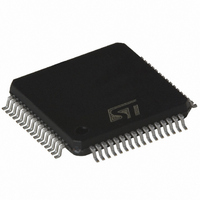
STLC5048TR STMicroelectronics, STLC5048TR Datasheet - Page 17

STLC5048TR
Manufacturer Part Number
STLC5048TR
Description
IC CODEC/FILTER PROGR 4CH 64TQFP
Manufacturer
STMicroelectronics
Type
PCM Codec/Filterr
Specifications of STLC5048TR
Data Interface
PCM Audio Interface
Resolution (bits)
16 b
Number Of Adcs / Dacs
4 / 4
Sigma Delta
Yes
Voltage - Supply, Analog
3.3 V ~ 5 V
Voltage - Supply, Digital
3.3 V ~ 5 V
Operating Temperature
-40°C ~ 85°C
Mounting Type
Surface Mount
Package / Case
64-TQFP, 64-VQFP
Lead Free Status / RoHS Status
Lead free / RoHS Compliant
Available stocks
Company
Part Number
Manufacturer
Quantity
Price
Company:
Part Number:
STLC5048TR
Manufacturer:
STMicroelectronics
Quantity:
10 000
STLC5048
4.8
VFRO output, referred to AGND must be AC coupled to the load, referred to VSS, to prevent
a DC current flow.
In order to get the best noise performances it is recommended to keep GRX value as close
as possible to the maximum (FFh) setting properly the additional attenuation by means of
RXG.
The intrinsic non programmable gain GR0 set the RX path gain to -3.15dB. The absolute
gain level (see
PCM interface
The STLC5048 dedicates eight pins to the interface with the PCM highways.
MCLK represents the bit clock and is also used by the device as a source for the clock of the
internal PLL.
Five possible frequencies can be used: 1.536/1.544 MHz (24-channel PCM frame);
2048 MHz (32-channel PCM frame); 4.096 MHz (64-channel PCM frame); 8.192 MHz (128
channels PCM frame). The operating frequency is automatically detected by the device the
first time both MCLK and FS are applied and becomes active after the second FS period.
MCLK synchronizes both the transmit data (DXA/B) and the receive data (DRA/B).
The Frame Synchronization signal FS is the common time base for all the four channels.
Transmit and receive programmable time-slots are framed by an internal synchronization
signal that can be coincident with FS or delayed of 1 or 7 MCLK cycles depending on the
programming of PCMSH register.
Two PCM ports are available: every channel can be connected to a different PCM port by
means of PCMCOM register.
DXA/B represents the transmit PCM interface. It remains in high impedance state except
during the assigned time slots during which the PCM data byte is shifted out on the
rising/falling edge of MCLK according to the TE bit of PCMCOM register. The four channels
can be shifted out in any possible time slot as defined by the DXTS registers. The assigned
time slot (transmit and receive) takes place in the 8 MCLK cycles following the rising edge of
FS.
The data can be shifted out on port A and/or B according to PCMCOM register.
If one codec is set in power down by software programming, the corresponding time slot is
set in high impedance. When linear coding mode is selected by CONF register
programming, the output channel will need two consecutive time slots (see
Register description
DRA/B represents the receive PCM interface. It remains inactive except during the assigned
time slots during which the PCM data byte is shifted in on the falling edge of MCLK. The four
channels are shifted in any possible time slot as defined by the DRTS registers.
If one codec is set in power down by software programming, the corresponding time slot is
not loaded and the VFRO output is kept at steady AGND level.
Chapter 9: Electrical characteristics
).
) refers to this intrinsic gain.
Functional description
Chapter 5:
17/64


