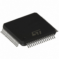
STLC5048TR STMicroelectronics, STLC5048TR Datasheet - Page 16

STLC5048TR
Manufacturer Part Number
STLC5048TR
Description
IC CODEC/FILTER PROGR 4CH 64TQFP
Manufacturer
STMicroelectronics
Type
PCM Codec/Filterr
Specifications of STLC5048TR
Data Interface
PCM Audio Interface
Resolution (bits)
16 b
Number Of Adcs / Dacs
4 / 4
Sigma Delta
Yes
Voltage - Supply, Analog
3.3 V ~ 5 V
Voltage - Supply, Digital
3.3 V ~ 5 V
Operating Temperature
-40°C ~ 85°C
Mounting Type
Surface Mount
Package / Case
64-TQFP, 64-VQFP
Lead Free Status / RoHS Status
Lead free / RoHS Compliant
Available stocks
Company
Part Number
Manufacturer
Quantity
Price
Company:
Part Number:
STLC5048TR
Manufacturer:
STMicroelectronics
Quantity:
10 000
Functional description
4.7
16/64
VFXI input must be AC coupled to the signal; the voltage swing allowed is 1.4 Vpp when the
preamplifier gain is set to 0 dB and 0.93 Vpp when the gain is 3.52 dB; higher levels must be
reduced through proper dividers.
Following the input amplifier the signal is converted into digital domain and a X filter block is
programmed to equalize together with the HPX and LPX filters the frequency response. The
coefficients of the X filter are programmed via the XFC command.
A gain block (GX) allows to set the transmit level in a 30 dB range, with steps <0.01 dB. This
block can be programmed via the GTX command.
The needed TX gain can be set by proper programming of the GX block in combination with
the TX amplifier.
Setting GTX=00h, the transmitted signal is muted and an idle PCM signal is generated on
DX.
Concerning the CODING function, A/m law can be selected writing the CONF register (bit 5
AMU). In addition, via the CONF register (bit 6 LIN) the coding law can be set to linear mode
(16 bits). In this case the signal sent on the DX will take two adjacent PCM channels, proper
care has to be taken in the time slot selection programming (DXTS register).
The intrinsic non-programmable gain GX0 set the TX path gain to 22.07 dB. The absolute
gain level (see
Receive path
The receive path of the STLC5048 consists of the decoder section, the gain block GR, the R
filter, the channel filters (LPR, HPR) the D/A converter and the output amplifier.
Concerning the DECODING function, A/m law can be selected writing the CONF register
(bit 5 AMU). In addition via the CONF register (bit 6 LIN) the coding law can be set to linear
mode (16 bits).
In this case the signal received on the DR input will take two adjacent PCM channels, proper
care has to be taken in the time slot selection programming (DRTS register).
The gain block GR is controlled by the GRX command allowing 30 dB gain range in 0.01 dB
steps.
The R filter together the channel filters (LPR and HPR) performs the line equalization. The
coefficients of the R filter are programmed via the RFC command.
The signal is converted in the analog domain and amplified by the RX amplifier that can be
programmed with four different values (mute, 0 dB, -6 dB and -12 dB) by means of RXG
register.
Figure 5.
DR
D00TL470
Receive path
A/μ
Chapter 9: Electrical characteristics
GR
GRO
) refers to this intrinsic gain.
CONV.
ΣΔ
for RXG=0dB; GR=0dB
0dBm0 => -3dBm/
RXG
600Ω
STLC5048
VFRO


