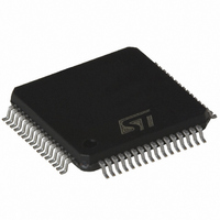
STLC5048TR STMicroelectronics, STLC5048TR Datasheet - Page 14

STLC5048TR
Manufacturer Part Number
STLC5048TR
Description
IC CODEC/FILTER PROGR 4CH 64TQFP
Manufacturer
STMicroelectronics
Type
PCM Codec/Filterr
Specifications of STLC5048TR
Data Interface
PCM Audio Interface
Resolution (bits)
16 b
Number Of Adcs / Dacs
4 / 4
Sigma Delta
Yes
Voltage - Supply, Analog
3.3 V ~ 5 V
Voltage - Supply, Digital
3.3 V ~ 5 V
Operating Temperature
-40°C ~ 85°C
Mounting Type
Surface Mount
Package / Case
64-TQFP, 64-VQFP
Lead Free Status / RoHS Status
Lead free / RoHS Compliant
Available stocks
Company
Part Number
Manufacturer
Quantity
Price
Company:
Part Number:
STLC5048TR
Manufacturer:
STMicroelectronics
Quantity:
10 000
Functional description
4
4.1
4.2
14/64
Functional description
The STLC5048 is a fully programmable device with embedded ROM and RAM. The ROM is
used to contain the default state coefficients for the programmable filters, while the RAM is
used to load the desired coefficient values.
When power is first applied it is recommended to reset the device (M1=M0=0) in order to set
all the internal registers to the reset value (see
also power down mode for all the four channels and SW reset bit (RES) set in the CONF
register.
When the RES bit is set, the only instructions allowed are the one that disable this bit and
the REACOM instruction: all other instructions are ignored. It is not possible to disable the
RES bit and write the other bits of the CONF register with the same instruction.
Of course, RESET mode can be programmed also by writing the RES bit of the CONF
register.
See
During RESET condition all the I/On and CSn pins are set as inputs, DX is in high
impedance and all VFROn are set to AGND. After the reset all registers are loaded with the
reset value.
It means that the PCM interface and all the VFRO outputs are configured as described in
the power down state, while no transmit or receive time slot are set.
Then, filters and gain blocks are configured with the coefficient defined in the default state.
Power down state
Each of the four channel may be put into power down mode by setting the appropriate bit in
the CONF register. In this mode the eventual programmed DX channel is set in high
impedance while the VFRO outputs are forced to AGND. When all the channels are set in
power down mode the device enters the power down state: all the blocks related to the data
processing are turned off, while the RAM is On or Off according to the PDR bit value in the
COMEN register.
Figure 3.
Power on initialization
Appendix C: Power sequences
DR
DX
* PROGRAMMABLE BLOCKS
A/mu
A/mu
Block diagram of a single channel
HPR
HPX
R
X
*
*
for the power up sequence.
GR
GX
*
*
B
*
Chapter 5: Register description
LPR
LPX
Z
*
KD
*
D/A
A/D
RX
TX
*
*
KA
D00TL468
; this means
*
STLC5048
VFRO
VFXI


