MC68EC020AA25 Freescale Semiconductor, MC68EC020AA25 Datasheet - Page 191
MC68EC020AA25
Manufacturer Part Number
MC68EC020AA25
Description
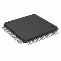
IC MPU 32BIT 25MHZ 100-QFP
Manufacturer
Freescale Semiconductor
Datasheet
1.MC68EC020AA16.pdf
(306 pages)
Specifications of MC68EC020AA25
Processor Type
M680x0 32-Bit
Speed
25MHz
Voltage
5V
Mounting Type
Surface Mount
Package / Case
100-QFP
Family Name
M68000
Device Core
ColdFire
Device Core Size
32b
Frequency (max)
25MHz
Instruction Set Architecture
RISC
Supply Voltage 1 (typ)
5V
Operating Supply Voltage (max)
5.25V
Operating Supply Voltage (min)
4.75V
Operating Temp Range
0C to 70C
Operating Temperature Classification
Commercial
Mounting
Surface Mount
Pin Count
100
Package Type
PQFP
Lead Free Status / RoHS Status
Lead free / RoHS Compliant
Features
-
Lead Free Status / Rohs Status
RoHS Compliant part
Electrostatic Device
Available stocks
Company
Part Number
Manufacturer
Quantity
Price
Company:

Part Number:
MC68EC020AA25
Manufacturer:
Freescale Semiconductor
Quantity:
10 000
Company:
Part Number:
MC68EC020AA25R
Manufacturer:
Freescale Semiconductor
Quantity:
10 000


The DR bit specifies the direction of the operand transfer. DR = 0 requests a transfer from
the main processor to the coprocessor, and DR = 1 specifies a transfer from the
coprocessor to the main processor.
If the effective addressing mode specifies the predecrement mode, the address register
used is decremented by the size of the operand before the transfer. The bytes within the
operand are then transferred to or from ascending addresses beginning with the location
specified by the decremented address register. In this mode, if A7 is used as the address
register and the operand length is one byte, A7 is decremented by two to maintain a word-
aligned stack.
For the postincrement effective addressing mode, the address register used is
incremented by the size of the operand after the transfer. The bytes within the operand
are transferred to or from ascending addresses beginning with the location specified by
the address register. In this mode, if A7 is used as the address register and the operand
length is one byte, A7 is incremented by two after the transfer to maintain a word-aligned
stack. Transferring odd length operands longer than one byte using the –(A7) or (A7)+
addressing modes can result in a stack pointer that is not word aligned.
The processor repeats the effective address calculation each time this primitive is issued
during the execution of a given instruction. The calculation uses the current contents of
any required address and data registers. The instruction must include a set of effective
address extension words for each repetition of a calculation that requires them. The
processor locates these words at the current scanPC location and increments the scanPC
by two for each word referenced in the instruction stream.
The MC68020/EC020 sign-extends a byte or word-sized operand to a long-word value
when it is transferred to an address register (A7–A0) using this primitive with the register
direct effective addressing mode. A byte or word-sized operand transferred to a data
register (D7–D0) only overwrites the lower byte or word of the data register.
7.4.10 Write to Previously Evaluated Effective Address Primitive
The write to previously evaluated effective address primitive transfers an operand from the
coprocessor to a previously evaluated effective address. This primitive applies to general
category instructions. If the coprocessor uses this primitive during the execution of a
conditional category instruction, the main processor initiates protocol violation exception
processing. Figure 7-30 shows the format of the write to previously evaluated effective
address primitive.
7-38
Figure 7-30. Write to Previously Evaluated Effective Address Primitive Format
15
CA
PC
14
13
1
12
0
11
0
10
0
M68020 USER’S MANUAL
9
0
8
0
7
LENGTH
MOTOROLA
0
Related parts for MC68EC020AA25
Image
Part Number
Description
Manufacturer
Datasheet
Request
R

Part Number:
Description:
Manufacturer:
Freescale Semiconductor, Inc
Datasheet:
Part Number:
Description:
Manufacturer:
Freescale Semiconductor, Inc
Datasheet:
Part Number:
Description:
Manufacturer:
Freescale Semiconductor, Inc
Datasheet:
Part Number:
Description:
Manufacturer:
Freescale Semiconductor, Inc
Datasheet:
Part Number:
Description:
Manufacturer:
Freescale Semiconductor, Inc
Datasheet:
Part Number:
Description:
Manufacturer:
Freescale Semiconductor, Inc
Datasheet:
Part Number:
Description:
Manufacturer:
Freescale Semiconductor, Inc
Datasheet:
Part Number:
Description:
Manufacturer:
Freescale Semiconductor, Inc
Datasheet:
Part Number:
Description:
Manufacturer:
Freescale Semiconductor, Inc
Datasheet:
Part Number:
Description:
Manufacturer:
Freescale Semiconductor, Inc
Datasheet:
Part Number:
Description:
Manufacturer:
Freescale Semiconductor, Inc
Datasheet:
Part Number:
Description:
Manufacturer:
Freescale Semiconductor, Inc
Datasheet:
Part Number:
Description:
Manufacturer:
Freescale Semiconductor, Inc
Datasheet:
Part Number:
Description:
Manufacturer:
Freescale Semiconductor, Inc
Datasheet:
Part Number:
Description:
Manufacturer:
Freescale Semiconductor, Inc
Datasheet: