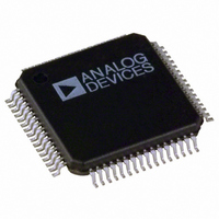
ADE7569ASTZF16 Analog Devices Inc, ADE7569ASTZF16 Datasheet - Page 145

ADE7569ASTZF16
Manufacturer Part Number
ADE7569ASTZF16
Description
IC ENERGY METER MCU 16K 64LQFP
Manufacturer
Analog Devices Inc
Specifications of ADE7569ASTZF16
Applications
Energy Measurement
Core Processor
8052
Program Memory Type
FLASH (16 kB)
Controller Series
ADE75xx
Ram Size
512 x 8
Interface
I²C, SPI, UART
Number Of I /o
20
Voltage - Supply
3.135 V ~ 3.465 V
Operating Temperature
-40°C ~ 85°C
Mounting Type
Surface Mount
Package / Case
64-LQFP
Ic Function
Single Phase Energy Measurement IC
Supply Voltage Range
3.13V To 3.46V, 2.4V To 3.7V
Operating Temperature Range
-40°C To +85°C
Digital Ic Case Style
LQFP
No. Of Pins
64
Lead Free Status / RoHS Status
Lead free / RoHS Compliant
Available stocks
Company
Part Number
Manufacturer
Quantity
Price
Company:
Part Number:
ADE7569ASTZF16
Manufacturer:
AD
Quantity:
310
Company:
Part Number:
ADE7569ASTZF16
Manufacturer:
Analog Devices Inc
Quantity:
10 000
Company:
Part Number:
ADE7569ASTZF16-RL
Manufacturer:
Analog Devices Inc
Quantity:
10 000
Table 163. Port 0 Alternate Functions
Pin No.
P0.0
P0.1
P0.2
P0.3
P0.4
P0.5
P0.6
P0.7
Table 164. Port 1 Alternate Functions
Pin No.
P1.0
P1.1
P1.2
P1.3
P1.4
P1.5
P1.6
P1.7
Table 165. Port 2 Alternate Functions
Pin No.
P2.0
P2.1
P2.2
P2.3
Alternate Function
BCTRL external battery control input
INT1 external interrupt
INT1 wake-up from PSM2 operating mode
FP19 LCD segment pin
CF1 ADE calibration frequency output
CF2 ADE calibration frequency output
MOSI SPI data line
SDATA I
MISO SPI data line
SCLK serial clock for I
T0 Timer 0 input
SS SPI slave select input for SPI in slave mode
SS SPI slave select output for SPI in master mode
T1 Timer 1 input
Alternate Function
RxD receiver data input for UART
Rx edge wake-up from PSM2 operating mode
TxD transmitter data output for UART
FP25 LCD segment pin
FP24 LCD segment pin
T2EX Timer 2 control input
FP23 LCD segment pin
T2 Timer 2 input
FP22 LCD segment pin
FP21 LCD segment pin
FP20 LCD segment pin
Alternate Function
FP18 LCD segment pin
FP17 LCD segment pin
FP16 LCD segment pin
SDEN serial download pin sampled on reset.
P2.3 is an output only.
2
C data line
2
C or SPI
ADE7116/ADE7156/ADE7166/ADE7169/ADE7566/ADE7569
Rev. B | Page 145 of 152
Alternate Function Enable
Set INT1PROG = X01 in the interrupt pins configuration SFR (INTPR,
Address 0xFF).
Set EX1 in the interrupt enable SFR (IE, Address 0xA8).
Address 0xFF).
Set FP19EN in the LCD Segment Enable 2 SFR (LCDSEGE2, Address 0xED).
Clear the DISCF1 bit in the ADE energy measurement internal MODE1
register (Address 0x0B).
Clear the DISCF2 bit in the ADE energy measurement internal MODE1
register (Address 0x0B).
Set the SCPS bit in the configuration SFR (CFG, Address 0xAF) and set the
SPIEN bit in the SPI configuration SFR 2 (SPIMOD2, Address 0xE9).
Clear the SCPS bit in the configuration SFR (CFG, Address 0xAF) and set the
I2CEN bit in the I
Set the SCPS bit in the configuration SFR (CFG, Address 0xAF) and set the
SPIEN bit in the SPI configuration SFR 2 (SPIMOD2, Address 0xE9).
Set the I2CEN bit in the I
in the SPI configuration SFR 2 (SPIMOD2, Address 0xE9) to enable the I
SPI interface.
Set the C/T0 bit in the Timer/Counter 0 and Timer/Counter 1 Mode SFR (TMOD,
Address 0x89) to enable T0 as an external event counter.
Set the SS_EN bit in the SPI configuration SFR 1 (SPIMOD1, Address 0xE8).
Set the SPIMS_b bit in the SPI configuration SFR 2 (SPIMOD2, Address 0xE9).
Set the C/T1 bit in the timer/counter 0 and timer/counter 1 mode SFR (TMOD,
Address 0x89) to enable T1 as an external event counter.
Alternate Function Enable
Set the REN bit in the serial communications control register bit description
SFR (SCON, Address 0x98).
Set RXPROG[1:0] = 11 in the peripheral configuration SFR (PERIPH, Address
0xF4).
This pin becomes TxD as soon as data is written into SBUF.
Set FP25EN in the LCD segment enable SFR (LCDSEGE, Address 0x97).
Set FP24EN in the LCD segment enable SFR (LCDSEGE, Address 0x97).
Set EXEN2 in the timer/counter 2 control SFR (T2CON, Address 0xC8).
Set FP23EN in the LCD segment enable SFR (LCDSEGE, Address 0x97).
Set the C/T2 bit in the timer/counter 2 control SFR (T2CON, Address 0xC8) to
enable T2 as an external event counter.
Set FP22EN in the LCD segment enable SFR (LCDSEGE, Address 0x97).
Set FP21EN in the LCD segment enable SFR (LCDSEGE, Address 0x97).
Set FP20EN in the LCD segment enable SFR (LCDSEGE, Address 0x97).
Alternate Function Enable
Set FP18EN in the LCD segment enable 2 SFR (LCDSEGE2, Address 0xED).
Set FP17EN in the LCD Segment enable 2 SFR (LCDSEGE2, Address 0xED).
Set FP16EN in the LCD segment enable 2 SFR (LCDSEGE2, Address 0xED).
Enabled by default.
Set INT1PROG = 11X in the interrupt pins configuration SFR (INTPR,
2
C Mode SFR (I2CMOD, Address 0xE8).
2
C Mode SFR (I2CMOD, Address 0xE8) or the SPIEN bit
2
C or


