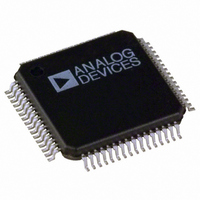
ADE7569ASTZF16 Analog Devices Inc, ADE7569ASTZF16 Datasheet - Page 100

ADE7569ASTZF16
Manufacturer Part Number
ADE7569ASTZF16
Description
IC ENERGY METER MCU 16K 64LQFP
Manufacturer
Analog Devices Inc
Specifications of ADE7569ASTZF16
Applications
Energy Measurement
Core Processor
8052
Program Memory Type
FLASH (16 kB)
Controller Series
ADE75xx
Ram Size
512 x 8
Interface
I²C, SPI, UART
Number Of I /o
20
Voltage - Supply
3.135 V ~ 3.465 V
Operating Temperature
-40°C ~ 85°C
Mounting Type
Surface Mount
Package / Case
64-LQFP
Ic Function
Single Phase Energy Measurement IC
Supply Voltage Range
3.13V To 3.46V, 2.4V To 3.7V
Operating Temperature Range
-40°C To +85°C
Digital Ic Case Style
LQFP
No. Of Pins
64
Lead Free Status / RoHS Status
Lead free / RoHS Compliant
Available stocks
Company
Part Number
Manufacturer
Quantity
Price
Company:
Part Number:
ADE7569ASTZF16
Manufacturer:
AD
Quantity:
310
Company:
Part Number:
ADE7569ASTZF16
Manufacturer:
Analog Devices Inc
Quantity:
10 000
Company:
Part Number:
ADE7569ASTZF16-RL
Manufacturer:
Analog Devices Inc
Quantity:
10 000
ADE7116/ADE7156/ADE7166/ADE7169/ADE7566/ADE7569
LCD DRIVER
Using shared pins, the LCD module is capable of directly driving
an LCD panel of 17 × 4 segments without compromising any
ADE7116/ADE7156/ADE7166/ADE7169/ADE7566/ADE7569
functions. It is capable of driving LCDs with 2×, 3×, and 4× multi-
plexing. The LCD waveform voltages generated through internal
charge pump circuitry support up to 5 V LCDs for the ADE7156/
ADE7166/ADE7169/ADE7566/ADE7569. An external resistor
ladder for LCD waveform voltage generation is also supported.
Each ADE7116/ADE7156/ADE7166/ADE7169/ADE7566/
ADE7569 has an embedded LCD control circuit, driver, and
power supply circuit. The LCD module is functional in all
operating modes (see the Operating Modes section).
Table 87. LCD Driver SFRs
SFR Address
0x95
0x96
0x97
0x9C
0xAC
0xAE
0xB1
0xED
Table 88. LCD Configuration SFR (LCDCON, Address 0x95)
Bit
7
6
5
4
3
2
[1:0]
Mnemonic
LCDEN
LCDRST
BLINKEN
LCDPSM2
CLKSEL
BIAS
LMUX
0
Default
0
0
0
0
0
0
R/W
R/W
R/W
R/W
R/W
R/W
R/W
R/W
R/W
Description
LCD enable. If this bit is set, the LCD driver is enabled.
LCD data registers reset. If this bit is set, the LCD data registers are reset to 0.
Blink mode enable bit. If this bit is set, blink mode is enabled. The blink mode is configured by the
BLKMOD and BLKFREQ bits in the LCD clock SFR (LCDCLK, Address 0x96).
Forces LCD off when in PSM2 (sleep) mode. Note that the internal voltage reference must be enabled by
setting the REF_BAT_EN bit in the Peripheral Configuration SFR (PERIPH, Address 0xF4) to allow LCD
operation in PSM2 mode.
LCDPSM2
0
1
LCD clock selection.
CLKSEL
0
1
Bias mode.
BIAS
0
1
LCD multiplex level.
LMUX
00
01
10
11
Mnemonic
LCDCON
LCDCLK
LCDSEGE
LCDCONX
LCDPTR
LCDDAT
LCDCONY
LCDSEGE2
Result
The LCD is disabled or enabled in PSM2 by the LCDEN bit
The LCD is disabled in PSM2 regardless of LCDEN setting
Result
f
f
Result
1/2
1/3
Result
Reserved.
2× multiplexing. FP27/COM3 is used as FP27, and FP28/COM2 is used as FP28.
3× multiplexing. FP27/COM3 is used as FP27, and FP28/COM2 is used as COM2.
4× multiplexing. FP27/COM3 is used as COM3, and FP28/COM2 is used as COM2.
LCDCLK
LCDCLK
= 2048 Hz
= 128 Hz
Rev. B | Page 100 of 152
Description
LCD configuration SFR (see Table 88).
LCD clock (see
Table 92).
LCD segment Enable (see Table 95).
LCD configuration X (see Table 89).
LCD pointer (see Table 96).
LCD data (see Table 97).
LCD configuration Y (see Table 91).
LCD segment Enable 2 (see Table 98).
LCD REGISTERS
There are six LCD control registers that configure the driver for
the specific type of LCD in the end system and set up the user
display preferences. The LCD configuration SFR (LCDCON,
Address 0x95), LCD Configuration X SFR (LCDCONX,
Address 0x9C), and LCD Configuration Y SFR (LCDCONY,
Address 0xB1) contain general LCD driver configuration
information including the LCD enable and reset, as well as the
method of LCD voltage generation and multiplex level. The
LCD clock SFR (LCDCLK, Address 0x96) configures timing
settings for LCD frame rate and blink rate. LCD pins are
configured for LCD functionality in the LCD segment enable
SFR (LCDSEGE, Address 0x97) and the LCD Segment Enable 2
SFR (LCDSEGE2, Address 0xED).


