DLP-HS-FPGA DLP Design Inc, DLP-HS-FPGA Datasheet - Page 9
DLP-HS-FPGA
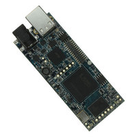
Manufacturer Part Number
DLP-HS-FPGA
Description
MODULE USB-TO-FPGA SPARTAN3
Manufacturer
DLP Design Inc
Datasheet
1.DLP-HS-FPGA.pdf
(17 pages)
Specifications of DLP-HS-FPGA
Module/board Type
FPGA Module
Interface Type
USB, SPI
Data Bus Width
32 bit
Operating Supply Voltage
5 V
Product
Interface Modules
For Use With/related Products
USB
Lead Free Status / RoHS Status
Lead free / RoHS Compliant
Lead Free Status / RoHS Status
Lead free / RoHS Compliant, Lead free / RoHS Compliant
Other names
813-1030
Available stocks
Company
Part Number
Manufacturer
Quantity
Price
Company:

Part Number:
DLP-HS-FPGA
Manufacturer:
DLP Design
Quantity:
135


Command
Rev. 1.1 (December 2009)
Read Pin
Clear Pin
Initialize
Memory
Memory
Memory
Packet
Set Pin
Read
Write
Description
Read the
state of one
of the User
I/O pins
Force the
selected
User I/O pin
low
Force the
selected
User I/O pin
high
Initialize
DDR2
SDRAM
Read 4
bytes from
DDR
SDRAM
Write 4
bytes to
DDR
SDRAM
Byte
0
1
0
1
0
1
0
0
1
2
3
0
1
2
3
4
5
6
7
Value Return/Comments
0xam
0xam
0x3E
0x3E
0x3E
0x30
0x00
0x40
0x00
0x41
0x00
0x70
0x8n
0xah
0x9n
0xah
0xd0
0xd1
0xd2
0xd3
Hex
0xal
0xal
TABLE 1 (continued)
–
–
–
Command Packets
Read Pin Command
The User I/O pin numbers are described in Table 2.
User I/O pin 0xnn is read and returns:
Clear Pin Command
The User I/O pin numbers are described in Table 2.
User I/O pin 0xnn is cleared. The specified user I/O
number is returned.
Set Pin Command
The User I/O pin numbers are described in Table 2.
User I/O pin 0xnn is set. The specified user I/O number
is returned.
The Initialize Memory command configures the DDR2
SDRAM for access by the FPGA. The memory cannot
be accessed without being initialized.
Read 4 bytes from the DDR2 SDRAM starting with the
address specified. The command byte is OR’d with the
Most Significant Address bit (24).
Bits 23 – 16 of the Address to be read from
Bits 15 – 8 of the Address to be read from
Bits 7 – 0 of the Address to be read from
Returns the 4 bytes read, followed by an echo back of
the command and address data sent.
NOTE: If the memory has not been initialized, the data
returned will be invalid and the command returned will
be 0xE7 indicating the error.
Write 4 bytes to the DDR2 SDRAM starting with the
address specified. The command byte is OR’d with the
Most Significant Address bit (24).
Bits 23 – 16 of the Address to be written to
Bits 15 – 8 of the Address to be written to
Bits 7 – 0 of the Address to be written to
Data Byte 0 written to Address specified
Data Byte 1 written to Address specified + 1
Data Byte 2 written to Address specified + 2
Data Byte 3 written to Address specified + 3
Returns the 4 bytes written, followed by an echo back of
the command and address data sent.
NOTE: If the memory has not been initialized, the
command returned will be 0xE7 indicating the error.
0x00 = User I/O pin 0xnn is low
0x01 = User I/O pin 0xnn is high
n = 0 the Most Significant Address bit is low (0x80)
n = 1 the most Significant Address bit is high (0x81)
n = 0 the Most Significant Address bit is low (0x90)
n = 1 the most Significant Address bit is high (0x91)
9
© DLP Design, Inc.
Related parts for DLP-HS-FPGA
Image
Part Number
Description
Manufacturer
Datasheet
Request
R

Part Number:
Description:
Interface Modules & Development Tools USB FPGA Module w/ Xilinx XC3S400A
Manufacturer:
DLP Design Inc
Datasheet:

Part Number:
Description:
MODULE USB-TO-UART/FIFO HS 18DIP
Manufacturer:
DLP Design Inc
Datasheet:

Part Number:
Description:
MODULE USB-TO-TTL SRL UART CONV
Manufacturer:
DLP Design Inc
Datasheet:

Part Number:
Description:
MODULE USB-TO-TTL PARL FIFO CONV
Manufacturer:
DLP Design Inc
Datasheet:
Part Number:
Description:
KIT DEV DLP LIGHTCOMANDER
Manufacturer:
Logic
Datasheet:

Part Number:
Description:
MODULE DATA-ACQUISITION 8-CH
Manufacturer:
DLP Design Inc
Datasheet:

Part Number:
Description:
MODULE DATA-ACQUISITION 20-CH
Manufacturer:
DLP Design Inc
Datasheet:

Part Number:
Description:
RFID READER/WRITER SNGL-CH OEM
Manufacturer:
DLP Design Inc
Datasheet:

Part Number:
Description:
Interface Modules & Development Tools DLP-245PL PACKAGED w/CCS Compiler
Manufacturer:
DLP Design Inc

Part Number:
Description:
MODULE USB-MCU FT245RL W/16F877A
Manufacturer:
DLP Design Inc
Datasheet:

Part Number:
Description:
MODULE USB-TO-FPGA TRAINING TOOL
Manufacturer:
DLP Design Inc
Datasheet:

Part Number:
Description:
MODULE USB-MCU FT232R W/18F2410
Manufacturer:
DLP Design Inc
Datasheet:

Part Number:
Description:
MODULE USB-MCU FT245RL W/SX48
Manufacturer:
DLP Design Inc
Datasheet:

Part Number:
Description:
MODULE USB-MCU FT2232D W/16F877A
Manufacturer:
DLP Design Inc
Datasheet:

Part Number:
Description:
MOD USB-MCU FT245RL W/18LF8722
Manufacturer:
DLP Design Inc
Datasheet: