DLP-HS-FPGA DLP Design Inc, DLP-HS-FPGA Datasheet - Page 2
DLP-HS-FPGA
Manufacturer Part Number
DLP-HS-FPGA
Description
MODULE USB-TO-FPGA SPARTAN3
Manufacturer
DLP Design Inc
Datasheet
1.DLP-HS-FPGA.pdf
(17 pages)
Specifications of DLP-HS-FPGA
Module/board Type
FPGA Module
Interface Type
USB, SPI
Data Bus Width
32 bit
Operating Supply Voltage
5 V
Product
Interface Modules
For Use With/related Products
USB
Lead Free Status / RoHS Status
Lead free / RoHS Compliant
Lead Free Status / RoHS Status
Lead free / RoHS Compliant, Lead free / RoHS Compliant
Other names
813-1030
Available stocks
Company
Part Number
Manufacturer
Quantity
Price
Company:

Part Number:
DLP-HS-FPGA
Manufacturer:
DLP Design
Quantity:
135


1.0 INTRODUCTION
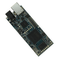
The DLP-HS-FPGA Module is a low-cost, compact prototyping module that can be used for rapid
proof of concept or for educational environments. The module is based on the Xilinx Spartan™ 3A
and Future Technology Devices International’s FT2232H Dual-Channel High Speed USB IC. The
DLP-HS-FPGA provides both the beginner as well as the experienced engineer with a rapid path to
developing FPGA-based designs. When combined with the free ISE™ WebPACK™ Tools from
Xilinx, this module is more than sufficient for creating anything from basic logical functions to a highly
complex system controller.
As a bonus feature, one channel of the dual-channel USB interface is used to load user bit files
directly to the SPI Flash—no external programmer is required. This represents a savings of as much
as $200 in that no additional programming cable is required for configuring the FPGA. All that is
needed to load bit files to the DLP-HS-FPGA is a Windows software utility (free with purchase), a
Windows PC and a USB cable. The module can also be programmed from within the Xilinx ISE tool
environment using a Xilinx programming cable (purchased separately).
The DLP-HS-FPGA is fully compatible with the free ISE™ WebPACK™ tools from Xilinx. ISE
WebPACK offers the ideal development environment for FPGA designs with HDL synthesis and
simulation, implementation, device fitting and JTAG programming.
The DLP-HS-FPGA has on-board voltage regulators that generate all required power supply voltages
from a single 5-volt source. Power for the module can be taken from either the host USB port or from
a user-supplied, external 5-volt power supply via an on board standard barrel connector.
Connection to user electronics is made via a 50-pin, 0.9-inch wide, industry-standard 0.025 square
inch post DIP header on the bottom of the board, and a 26 pin, 0.05 inch wide top side 2x13 header.
The bottom side 50 pin header provides access to 41 of the FPGA user input/output pins. The top
side header provides access to 22 of the FPGA user input/output pins. The bottom side header mates
with a user supplied standard 50 pin 0.9 inch spaced DIP socket. The top side header mates with a
user supplied 0.05 inch spaced 2x13 connector such as the FFSD-13-D-xx.xx-01 (xx.xx = cable
length) ribbon cable assembly from Samtec.
DIP Socket
Ribbon Cable
Other on-board features include a 32M x 8 DDR2 SDRAM memory IC for user projects, and both
JTAG and SPI Flash interface ports for connection to Xilinx programming tools.
Rev. 1.1 (December 2009)
2
© DLP Design, Inc.
Related parts for DLP-HS-FPGA
Image
Part Number
Description
Manufacturer
Datasheet
Request
R

Part Number:
Description:
Interface Modules & Development Tools USB FPGA Module w/ Xilinx XC3S400A
Manufacturer:
DLP Design Inc
Datasheet:

Part Number:
Description:
MODULE USB-TO-UART/FIFO HS 18DIP
Manufacturer:
DLP Design Inc
Datasheet:

Part Number:
Description:
MODULE USB-TO-TTL SRL UART CONV
Manufacturer:
DLP Design Inc
Datasheet:

Part Number:
Description:
MODULE USB-TO-TTL PARL FIFO CONV
Manufacturer:
DLP Design Inc
Datasheet:
Part Number:
Description:
KIT DEV DLP LIGHTCOMANDER
Manufacturer:
Logic
Datasheet:

Part Number:
Description:
MODULE DATA-ACQUISITION 8-CH
Manufacturer:
DLP Design Inc
Datasheet:

Part Number:
Description:
MODULE DATA-ACQUISITION 20-CH
Manufacturer:
DLP Design Inc
Datasheet:

Part Number:
Description:
RFID READER/WRITER SNGL-CH OEM
Manufacturer:
DLP Design Inc
Datasheet:

Part Number:
Description:
Interface Modules & Development Tools DLP-245PL PACKAGED w/CCS Compiler
Manufacturer:
DLP Design Inc

Part Number:
Description:
MODULE USB-MCU FT245RL W/16F877A
Manufacturer:
DLP Design Inc
Datasheet:

Part Number:
Description:
MODULE USB-TO-FPGA TRAINING TOOL
Manufacturer:
DLP Design Inc
Datasheet:

Part Number:
Description:
MODULE USB-MCU FT232R W/18F2410
Manufacturer:
DLP Design Inc
Datasheet:

Part Number:
Description:
MODULE USB-MCU FT245RL W/SX48
Manufacturer:
DLP Design Inc
Datasheet:

Part Number:
Description:
MODULE USB-MCU FT2232D W/16F877A
Manufacturer:
DLP Design Inc
Datasheet:

Part Number:
Description:
MOD USB-MCU FT245RL W/18LF8722
Manufacturer:
DLP Design Inc
Datasheet: