DLP-HS-FPGA DLP Design Inc, DLP-HS-FPGA Datasheet - Page 11
DLP-HS-FPGA
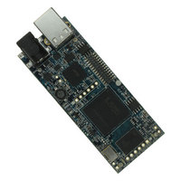
Manufacturer Part Number
DLP-HS-FPGA
Description
MODULE USB-TO-FPGA SPARTAN3
Manufacturer
DLP Design Inc
Datasheet
1.DLP-HS-FPGA.pdf
(17 pages)
Specifications of DLP-HS-FPGA
Module/board Type
FPGA Module
Interface Type
USB, SPI
Data Bus Width
32 bit
Operating Supply Voltage
5 V
Product
Interface Modules
For Use With/related Products
USB
Lead Free Status / RoHS Status
Lead free / RoHS Compliant
Lead Free Status / RoHS Status
Lead free / RoHS Compliant, Lead free / RoHS Compliant
Other names
813-1030
Available stocks
Company
Part Number
Manufacturer
Quantity
Price
Company:

Part Number:
DLP-HS-FPGA
Manufacturer:
DLP Design
Quantity:
135


Rev. 1.1 (December 2009)
I/O Number
+3.3V OUT
SUSPEND
0x2C (44)
0x2D (45)
0x3C (60)
0x3D (61)
0x2A (42)
0x2B (43)
0x2E (46)
0x2F (47)
0x3A (58)
0x3B (59)
0x3E (62)
0x24 (36)
0x25 (37)
0x26 (38)
0x27 (39)
0x28 (40)
0x29 (41)
0x30 (48)
0x31 (49)
0x32 (50)
0x33 (51)
0x34 (52)
0x35 (53)
0x36 (54)
0x37 (55)
0x38 (56)
0x39 (57)
+5V USB
AWAKE
+5V IN
GND
FPGA Pin
J1 pin 28,
J1 pin 11,
J1 pin 25,
J1 pin 26,
J1 pin 40,
J1 pin 50,
DLP-HS-
J1 pin 45
J1 pin 46
J1 pin 47
J1 pin 48
J1 pin 49
J4 pin 11
J4 pin 13
J4 pin 15
J4 pin 17
J4 pin 19
J4 pin 21
J4 pin 10
J4 pin 12
J4 pin 14
J4 pin 16
J4 pin 18
J4 pin 20
J4 pin 22
J4 pin 23
J4 pin 24
J1 pin 23
J1 pin 24
J4 pin 26
J4 pin 25
J1 pin 1,
J4 pin 1
J4 pin 3
J4 pin 5
J4 pin 7
J4 pin 9
J4 pin 2
J4 pin 4
J4 pin 6
J4 pin 8
XC3S200A
B15
A12
B10
A10
R16
T11
Pin
M1
M3
N2
N1
C4
C7
R1
G1
H1
K1
K3
P1
T9
A9
E7
K4
A7
A4
B4
F1
J1
L1
L4
-
-
-
-
TABLE 2 (Continued)
XC3S200A
User I/O
Bank
3
3
3
3
2
0
0
0
0
0
3
0
0
0
3
3
0
0
0
3
3
3
3
3
3
3
3
1
2
-
-
-
-
11
FPGA Pin Configurations available
Digital Input, Output, Differential Pair 18-,
Regional Clock
Digital Input, Output, Differential Pair 18+,
Regional Clock
Digital Input, Output, Differential Pair 19-
Digital Input, Output, Differential Pair 19+
Digital Input, Output, Global Clock
Digital Input, Output
Digital Input, Output
Digital Input, Output, Differential Pair 20+
Digital Input, Output, Differential Pair 20-
Digital Input, Output, Global Clock
Digital Input, Output
Digital Input, Output
Digital Input, Output
Digital Input, Output
Digital Input, Output
Digital Input, Output
Digital Input, Output
Digital Input, Output, Differential Pair 21+
Digital Input, Output, Differential Pair 21-
Digital Input, Output, Differential Pair 22+
Digital Input, Output, Differential Pair 22-
Digital Input, Output, Regional Clock
Digital Input, Output, Regional Clock
Digital Input, Output
Digital Input, Output
Digital Input, Output, Differential Pair 23+
Digital Input, Output, Differential Pair 23-
Force Suspend Mode (when enabled)
Return from Suspend Mode operation
+5V input to the DLP-HS-FPGA
+5V supplied by Host PC USB Port
+3.3V supplied by on board DLP-HS-
FPGA regulator after module enumerated
Ground
© DLP Design, Inc.
Related parts for DLP-HS-FPGA
Image
Part Number
Description
Manufacturer
Datasheet
Request
R

Part Number:
Description:
Interface Modules & Development Tools USB FPGA Module w/ Xilinx XC3S400A
Manufacturer:
DLP Design Inc
Datasheet:

Part Number:
Description:
MODULE USB-TO-UART/FIFO HS 18DIP
Manufacturer:
DLP Design Inc
Datasheet:

Part Number:
Description:
MODULE USB-TO-TTL SRL UART CONV
Manufacturer:
DLP Design Inc
Datasheet:

Part Number:
Description:
MODULE USB-TO-TTL PARL FIFO CONV
Manufacturer:
DLP Design Inc
Datasheet:
Part Number:
Description:
KIT DEV DLP LIGHTCOMANDER
Manufacturer:
Logic
Datasheet:

Part Number:
Description:
MODULE DATA-ACQUISITION 8-CH
Manufacturer:
DLP Design Inc
Datasheet:

Part Number:
Description:
MODULE DATA-ACQUISITION 20-CH
Manufacturer:
DLP Design Inc
Datasheet:

Part Number:
Description:
RFID READER/WRITER SNGL-CH OEM
Manufacturer:
DLP Design Inc
Datasheet:

Part Number:
Description:
Interface Modules & Development Tools DLP-245PL PACKAGED w/CCS Compiler
Manufacturer:
DLP Design Inc

Part Number:
Description:
MODULE USB-MCU FT245RL W/16F877A
Manufacturer:
DLP Design Inc
Datasheet:

Part Number:
Description:
MODULE USB-TO-FPGA TRAINING TOOL
Manufacturer:
DLP Design Inc
Datasheet:

Part Number:
Description:
MODULE USB-MCU FT232R W/18F2410
Manufacturer:
DLP Design Inc
Datasheet:

Part Number:
Description:
MODULE USB-MCU FT245RL W/SX48
Manufacturer:
DLP Design Inc
Datasheet:

Part Number:
Description:
MODULE USB-MCU FT2232D W/16F877A
Manufacturer:
DLP Design Inc
Datasheet:

Part Number:
Description:
MOD USB-MCU FT245RL W/18LF8722
Manufacturer:
DLP Design Inc
Datasheet: