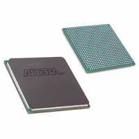
EP1SGX25CF672C6 Altera, EP1SGX25CF672C6 Datasheet - Page 9

EP1SGX25CF672C6
Manufacturer Part Number
EP1SGX25CF672C6
Description
IC STRATIX GX FPGA 25KLE 672FBGA
Manufacturer
Altera
Series
Stratix® GXr
Datasheet
1.EP1SGX10CF672C7N.pdf
(272 pages)
Specifications of EP1SGX25CF672C6
Number Of Logic Elements/cells
25660
Number Of Labs/clbs
2566
Total Ram Bits
1944576
Number Of I /o
455
Voltage - Supply
1.425 V ~ 1.575 V
Mounting Type
Surface Mount
Operating Temperature
0°C ~ 85°C
Package / Case
672-FBGA
Family Name
Stratix GX
Number Of Logic Blocks/elements
25660
# I/os (max)
455
Frequency (max)
5GHz
Process Technology
SRAM
Operating Supply Voltage (typ)
1.5V
Logic Cells
25660
Ram Bits
1944576
Operating Supply Voltage (min)
1.425V
Operating Supply Voltage (max)
1.575V
Operating Temp Range
0C to 85C
Operating Temperature Classification
Commercial
Mounting
Surface Mount
Pin Count
672
Package Type
FC-FBGA
Lead Free Status / RoHS Status
Contains lead / RoHS non-compliant
Number Of Gates
-
Lead Free Status / Rohs Status
Not Compliant
Available stocks
Company
Part Number
Manufacturer
Quantity
Price
Company:
Part Number:
EP1SGX25CF672C6
Manufacturer:
ALTERA
Quantity:
3 000
Part Number:
EP1SGX25CF672C6
Manufacturer:
ALTERA/阿尔特拉
Quantity:
20 000
Company:
Part Number:
EP1SGX25CF672C6ES
Manufacturer:
ALTERA
Quantity:
5
Figure 1–2. Stratix GX Block Diagram
Altera Corporation
February 2005
EP1SGX10
EP1SGX25
EP1SGX40
Table 1–5. Stratix GX Device Resources
IOEs
IOEs
IOEs
IOEs
IOEs
IOEs
IOEs
IOEs
IOEs
IOEs
IOEs
IOEs
IOEs
IOEs
IOEs
IOEs
IOEs
Device
IOEs
LABs
LABs
LABs
LABs
LABs
LABs
LABs
LABs
LABs
LABs
LABs
LABs
LABs
LABs
LABs
LABs
LABs
Columns/Blocks
M512 RAM
M512 RAM Blocks for
Dual-Port Memory, Shift
Registers, & FIFO Buffers
6 / 224
8 / 384
4 / 94
IOEs
LABs
LABs
LABs
LABs
LABs
LABs
LABs
LABs
LABs
LABs
LABs
LABs
LABs
LABs
LABs
LABs
LABs
The number of M512 RAM, M4K RAM, and DSP blocks varies by device
along with row and column numbers and M-RAM blocks.
the resources available in Stratix GX devices.
Columns/Blocks
DSP
Block
M4K RAM
DSP Blocks for
Multiplication and Full
Implementation of FIR Filters
3 / 138
3 / 183
2 / 60
LABs
LABs
LABs
LABs
LABs
LABs
LABs
LABs
LABs
LABs
LABs
LABs
LABs
LABs
LABs
LABs
LABs
IOEs
M-RAM
Blocks
M4K RAM Blocks
for True Dual-Port
Memory & Other Embedded
Memory Functions
1
2
4
Introduction to the Stratix GX Device Data Sheet
LABs
LABs
LABs
LABs
LABs
LABs
LABs
LABs
LABs
LABs
LABs
LABs
LABs
LABs
LABs
LABs
LABs
Columns/Blocks
DSP Block
IOEs Support DDR, PCI, GTL+, SSTL-3,
SSTL-2, HSTL, LVDS, LVPECL, PCML,
HyperTransport & other I/O Standards
Stratix GX Device Handbook, Volume 1
2 / 10
2 / 14
2 / 6
LABs
LABs
LABs
LABs
LABs
IOEs
M-RAM Block
Columns
LAB
40
62
77
LABs
LABs
LABs
LABs
LABs
Table 1–5
LAB Rows
30
46
61
lists
1–7


