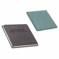
EP1SGX25CF672C6 Altera, EP1SGX25CF672C6 Datasheet - Page 186

EP1SGX25CF672C6
Manufacturer Part Number
EP1SGX25CF672C6
Description
IC STRATIX GX FPGA 25KLE 672FBGA
Manufacturer
Altera
Series
Stratix® GXr
Datasheet
1.EP1SGX10CF672C7N.pdf
(272 pages)
Specifications of EP1SGX25CF672C6
Number Of Logic Elements/cells
25660
Number Of Labs/clbs
2566
Total Ram Bits
1944576
Number Of I /o
455
Voltage - Supply
1.425 V ~ 1.575 V
Mounting Type
Surface Mount
Operating Temperature
0°C ~ 85°C
Package / Case
672-FBGA
Family Name
Stratix GX
Number Of Logic Blocks/elements
25660
# I/os (max)
455
Frequency (max)
5GHz
Process Technology
SRAM
Operating Supply Voltage (typ)
1.5V
Logic Cells
25660
Ram Bits
1944576
Operating Supply Voltage (min)
1.425V
Operating Supply Voltage (max)
1.575V
Operating Temp Range
0C to 85C
Operating Temperature Classification
Commercial
Mounting
Surface Mount
Pin Count
672
Package Type
FC-FBGA
Lead Free Status / RoHS Status
Contains lead / RoHS non-compliant
Number Of Gates
-
Lead Free Status / Rohs Status
Not Compliant
Available stocks
Company
Part Number
Manufacturer
Quantity
Price
Company:
Part Number:
EP1SGX25CF672C6
Manufacturer:
ALTERA
Quantity:
3 000
Part Number:
EP1SGX25CF672C6
Manufacturer:
ALTERA/阿尔特拉
Quantity:
20 000
Company:
Part Number:
EP1SGX25CF672C6ES
Manufacturer:
ALTERA
Quantity:
5
I/O Structure
4–120
Stratix GX Device Handbook, Volume 1
Notes to
(1)
(2)
(3)
R
Table 4–31. Differential On-Chip Termination
Symbol
D
(2)
Data measured over minimum conditions (T
V
Data measured over minimum conditions (T
V
LVDS data rate is supported for 840 Mbps using internal differential termination.
CCIO
CCIO
Table
= –5%).
= –5%).
Internal differential termination for LVDS
4–31:
Description
However, there is additional resistance present between the device ball
and the input of the receiver buffer, as shown in
resistance is because of package trace resistance (which can be calculated
as the resistance from the package ball to the pad) and the parasitic layout
metal routing resistance (which is shown between the pad and the
intersection of the on-chip termination and input buffer).
Figure 4–71. Differential Resistance of LVDS Differential Pin Pair (R
Table 4–31
commercial devices.
MultiVolt I/O Interface
The Stratix GX architecture supports the MultiVolt I/O interface feature,
which allows Stratix GX devices in all packages to interface with systems
of different supply voltages.
The Stratix GX VCCINT pins must always be connected to a 1.5-V power
supply. With a 1.5-V V
3.3-V tolerant. The VCCIO pins can be connected to either a 1.5-V, 1.8-V,
defines the specification for internal termination resistance for
Package Ball
Package Ball
R
D
j
j
= –40 C, V
= 0 C, V
0.3 Ω
0.3 Ω
CCINT
C C I O
CCIO
Pad
Pad
Commercial (1),
Industrial (2),
+5%) and maximum conditions (T
+5%) and maximum conditions (T
level, input pins are 1.5-V, 1.8-V, 2.5-V, and
9.3 Ω
9.3 Ω
Conditions
(3)
(3)
Input Buffer
LVDS
Differential On-Chip
Termination Resistor
Figure
Min
110
100
Resistance
Altera Corporation
4–71. This
j
135
135
Typ
= 85 C,
j
= 100 C,
February 2005
Max
165
170
D
)
Unit
Ω
Ω


