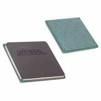
EP1SGX25CF672C6 Altera, EP1SGX25CF672C6 Datasheet - Page 224

EP1SGX25CF672C6
Manufacturer Part Number
EP1SGX25CF672C6
Description
IC STRATIX GX FPGA 25KLE 672FBGA
Manufacturer
Altera
Series
Stratix® GXr
Datasheet
1.EP1SGX10CF672C7N.pdf
(272 pages)
Specifications of EP1SGX25CF672C6
Number Of Logic Elements/cells
25660
Number Of Labs/clbs
2566
Total Ram Bits
1944576
Number Of I /o
455
Voltage - Supply
1.425 V ~ 1.575 V
Mounting Type
Surface Mount
Operating Temperature
0°C ~ 85°C
Package / Case
672-FBGA
Family Name
Stratix GX
Number Of Logic Blocks/elements
25660
# I/os (max)
455
Frequency (max)
5GHz
Process Technology
SRAM
Operating Supply Voltage (typ)
1.5V
Logic Cells
25660
Ram Bits
1944576
Operating Supply Voltage (min)
1.425V
Operating Supply Voltage (max)
1.575V
Operating Temp Range
0C to 85C
Operating Temperature Classification
Commercial
Mounting
Surface Mount
Pin Count
672
Package Type
FC-FBGA
Lead Free Status / RoHS Status
Contains lead / RoHS non-compliant
Number Of Gates
-
Lead Free Status / Rohs Status
Not Compliant
Available stocks
Company
Part Number
Manufacturer
Quantity
Price
Company:
Part Number:
EP1SGX25CF672C6
Manufacturer:
ALTERA
Quantity:
3 000
Part Number:
EP1SGX25CF672C6
Manufacturer:
ALTERA/阿尔特拉
Quantity:
20 000
Company:
Part Number:
EP1SGX25CF672C6ES
Manufacturer:
ALTERA
Quantity:
5
Power Consumption
Power
Consumption
Timing Model
6–22
Stratix GX Device Handbook, Volume 1
Notes to
(1)
(2)
V
V
I
Low sustaining
current
High sustaining
current
Low overdrive
current
High overdrive
current
Bus-hold trip
point
O
Table 6–32. CTT I/O Specifications (Part 2 of 2)
Table 6–33. Bus Hold Parameters
OH
OL
Parameter
Symbol
Drive strength is programmable according to values in the Stratix GX Architecture chapter of the Stratix GX Device
Handbook, Volume 1.
V
R E F
Tables 6–14
specifies the center point of the switching range.
High-level output voltage
Low-level output voltage
Output leakage current
(when output is high Z)
V
(maximum)
V
(minimum)
0 V < V
V
0 V < V
V
Conditions
IN
IN
CCIO
CCIO
through 6–33:
> V
< V
Parameter
IL
IH
IN
IN
<
<
Detailed power consumption information for Stratix GX devices will be
released when available.
The DirectDrive
predictable performance, accurate simulation, and accurate timing
analysis across all Stratix GX device densities and speed grades. This
section describes and specifies the performance, internal, external, and
PLL timing specifications.
All specifications are representative of worst-case supply voltage and
junction temperature conditions.
Min
–25
0.5
25
1.5 V
–160
Max
160
I
I
GND ≤ V
V
1.0
OH
OL
C C I O
Conditions
= 8 mA
= –8 mA
™
technology and MultiTrack
O U T
0.68
Min
–30
30
1.8 V
≤
–200
Max
1.07
200
V
–10
V
Minimum
R E F
C C I O
+ 0.4
Level
Min
–50
0.7
50
2.5 V
Typical
–300
Max
300
1.7
™
interconnect ensure
V
10
Min
–70
Maximum
0.8
70
R E F
Altera Corporation
3.3 V
– 0.4
–500
Max
500
2.0
June 2006
Units
μA
Units
V
V
μA
μA
μA
μA
V


