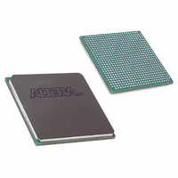
EP1SGX25CF672C6 Altera, EP1SGX25CF672C6 Datasheet - Page 225

EP1SGX25CF672C6
Manufacturer Part Number
EP1SGX25CF672C6
Description
IC STRATIX GX FPGA 25KLE 672FBGA
Manufacturer
Altera
Series
Stratix® GXr
Datasheet
1.EP1SGX10CF672C7N.pdf
(272 pages)
Specifications of EP1SGX25CF672C6
Number Of Logic Elements/cells
25660
Number Of Labs/clbs
2566
Total Ram Bits
1944576
Number Of I /o
455
Voltage - Supply
1.425 V ~ 1.575 V
Mounting Type
Surface Mount
Operating Temperature
0°C ~ 85°C
Package / Case
672-FBGA
Family Name
Stratix GX
Number Of Logic Blocks/elements
25660
# I/os (max)
455
Frequency (max)
5GHz
Process Technology
SRAM
Operating Supply Voltage (typ)
1.5V
Logic Cells
25660
Ram Bits
1944576
Operating Supply Voltage (min)
1.425V
Operating Supply Voltage (max)
1.575V
Operating Temp Range
0C to 85C
Operating Temperature Classification
Commercial
Mounting
Surface Mount
Pin Count
672
Package Type
FC-FBGA
Lead Free Status / RoHS Status
Contains lead / RoHS non-compliant
Number Of Gates
-
Lead Free Status / Rohs Status
Not Compliant
Available stocks
Company
Part Number
Manufacturer
Quantity
Price
Company:
Part Number:
EP1SGX25CF672C6
Manufacturer:
ALTERA
Quantity:
3 000
Part Number:
EP1SGX25CF672C6
Manufacturer:
ALTERA/阿尔特拉
Quantity:
20 000
Company:
Part Number:
EP1SGX25CF672C6ES
Manufacturer:
ALTERA
Quantity:
5
Altera Corporation
June 2006
LE
Table 6–35. Stratix GX Device Performance (Part 1 of 3)
16-to-1 multiplexer
32-to-1 multiplexer
16-bit counter
64-bit counter
Applications
Preliminary & Final Timing
Timing models can have either preliminary or final status. The
Quartus
design compilation if the timing models are preliminary.
shows the status of the Stratix GX device timing models.
Preliminary status means the timing model is subject to change. Initially,
timing numbers are created using simulation results, process data, and
other known parameters. These tests are used to make the preliminary
numbers as close to the actual timing parameters as possible.
Final timing numbers are based on actual device operation and testing.
These numbers reflect the actual performance of the device under
worst-case voltage and junction temperature conditions.
Performance
Table 6–35
designs. All performance values were obtained with Quartus II software
compilation of LPM, or MegaCore
designs.
EP1SGX10
EP1SGX25
EP1SGX40
Table 6–34. Stratix GX Device Timing Model Status
(1)
(3)
®
Device
II software displays an informational message during the
shows Stratix GX device performance for some common
LEs
22
46
16
64
Resources Used
TriMatrix
Memory
Blocks
0
0
0
0
Preliminary
Notes
Blocks
DSP
0
0
0
0
®
—
—
—
Stratix GX Device Handbook, Volume 1
functions for the FIR and FFT
(1),
407.83
318.26
422.11
321.85
Speed
Grade
(2)
-5
DC & Switching Characteristics
324.56
255.29
422.11
290.52
Speed
Grade
Performance
-6
288.68
242.89
390.01
261.23
Table 6–34
Speed
Grade
Final
-7
v
v
v
Units
MHz
MHz
MHz
MHz
6–23


