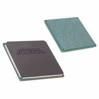
EP1SGX25CF672C6 Altera, EP1SGX25CF672C6 Datasheet - Page 110

EP1SGX25CF672C6
Manufacturer Part Number
EP1SGX25CF672C6
Description
IC STRATIX GX FPGA 25KLE 672FBGA
Manufacturer
Altera
Series
Stratix® GXr
Datasheet
1.EP1SGX10CF672C7N.pdf
(272 pages)
Specifications of EP1SGX25CF672C6
Number Of Logic Elements/cells
25660
Number Of Labs/clbs
2566
Total Ram Bits
1944576
Number Of I /o
455
Voltage - Supply
1.425 V ~ 1.575 V
Mounting Type
Surface Mount
Operating Temperature
0°C ~ 85°C
Package / Case
672-FBGA
Family Name
Stratix GX
Number Of Logic Blocks/elements
25660
# I/os (max)
455
Frequency (max)
5GHz
Process Technology
SRAM
Operating Supply Voltage (typ)
1.5V
Logic Cells
25660
Ram Bits
1944576
Operating Supply Voltage (min)
1.425V
Operating Supply Voltage (max)
1.575V
Operating Temp Range
0C to 85C
Operating Temperature Classification
Commercial
Mounting
Surface Mount
Pin Count
672
Package Type
FC-FBGA
Lead Free Status / RoHS Status
Contains lead / RoHS non-compliant
Number Of Gates
-
Lead Free Status / Rohs Status
Not Compliant
Available stocks
Company
Part Number
Manufacturer
Quantity
Price
Company:
Part Number:
EP1SGX25CF672C6
Manufacturer:
ALTERA
Quantity:
3 000
Part Number:
EP1SGX25CF672C6
Manufacturer:
ALTERA/阿尔特拉
Quantity:
20 000
Company:
Part Number:
EP1SGX25CF672C6ES
Manufacturer:
ALTERA
Quantity:
5
TriMatrix Memory
Figure 4–25. Input/Output Clock Mode in Simple Dual-Port Mode
Note to
(1)
4–44
Stratix GX Device Handbook, Volume 1
All registers shown except the rden register have asynchronous clear ports.
Figure
wraddress[ ]
address[ ]
byteena[ ]
outclken
wrclock
inclken
rdclock
data[ ]
wren
rden
4–25:
8 LAB Row
Clocks
8
Read/Write Clock Mode
The memory blocks implement read/write clock mode for simple dual-
port memory. You can use up to two clocks in this mode. The write clock
controls the block’s data inputs, wraddress, and wren. The read clock
controls the data output, rdaddress, and rden. The memory blocks
support independent clock enables for each clock and asynchronous clear
signals for the read- and write-side registers.
memory block in read/write clock mode.
D
ENA
D
ENA
D
ENA
D
ENA
D
ENA
D
ENA
Q
Q
Q
Q
Q
Q
Generator
Pulse
Write
Data In
Read Address
Byte Enable
Write Address
Read Enable
Write Enable
Memory Block
Data Out
1,024 ´ 4
2,048 ´ 2
4,096 ´ 1
256 ´ 16
512 ´ 8
Note (1)
D
ENA
Figure 4–26
Q
Altera Corporation
To MultiTrack
Interconnect
shows a
February 2005


