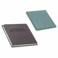
EP1SGX25CF672C6 Altera, EP1SGX25CF672C6 Datasheet - Page 185

EP1SGX25CF672C6
Manufacturer Part Number
EP1SGX25CF672C6
Description
IC STRATIX GX FPGA 25KLE 672FBGA
Manufacturer
Altera
Series
Stratix® GXr
Datasheet
1.EP1SGX10CF672C7N.pdf
(272 pages)
Specifications of EP1SGX25CF672C6
Number Of Logic Elements/cells
25660
Number Of Labs/clbs
2566
Total Ram Bits
1944576
Number Of I /o
455
Voltage - Supply
1.425 V ~ 1.575 V
Mounting Type
Surface Mount
Operating Temperature
0°C ~ 85°C
Package / Case
672-FBGA
Family Name
Stratix GX
Number Of Logic Blocks/elements
25660
# I/os (max)
455
Frequency (max)
5GHz
Process Technology
SRAM
Operating Supply Voltage (typ)
1.5V
Logic Cells
25660
Ram Bits
1944576
Operating Supply Voltage (min)
1.425V
Operating Supply Voltage (max)
1.575V
Operating Temp Range
0C to 85C
Operating Temperature Classification
Commercial
Mounting
Surface Mount
Pin Count
672
Package Type
FC-FBGA
Lead Free Status / RoHS Status
Contains lead / RoHS non-compliant
Number Of Gates
-
Lead Free Status / Rohs Status
Not Compliant
Available stocks
Company
Part Number
Manufacturer
Quantity
Price
Company:
Part Number:
EP1SGX25CF672C6
Manufacturer:
ALTERA
Quantity:
3 000
Part Number:
EP1SGX25CF672C6
Manufacturer:
ALTERA/阿尔特拉
Quantity:
20 000
Company:
Part Number:
EP1SGX25CF672C6ES
Manufacturer:
ALTERA
Quantity:
5
Altera Corporation
February 2005
Notes to
(1)
(2)
Differential termination (1),
Table 4–29. Differential Termination Supported by I/O Banks
Differential Termination Support
Clock pin CLK0, CLK2, CLK9, CLK11, and pins FPLL[7..10]CLK do not support differential termination.
Differential termination is only supported for LVDS because of a 3.3-V V
Table
4–29:
(2)
Figure 4–70. LVDS Input Differential On-Chip Termination
I/O banks on the left and right side of the device support LVDS receiver
(far-end) differential termination.
Table 4–29
Table 4–30
The differential on-chip resistance at the receiver input buffer is
118
Top and bottom I/O banks (3, 4, 7, and 8)
DIFFIO_RX[]
CLK[0,2,9,11],CLK[4-7],CLK[12-15]
CLK[1,3,8,10]
FCLK
FPLL[7..10]CLK
Table 4–30. Differential Termination Support Across Pin Types
Ω ±
20 %.
I/O Standard Support
Transmitting
shows the Stratix GX device differential termination support.
shows the termination support for different pin types.
Device
+
Ð
LVDS
Pin Type
Banks (3, 4, 7 & 8)
Z
Z
Top & Bottom
0
0
Stratix GX Device Handbook, Volume 1
C C I O
.
Differential Termination
Receiving Device with
R
D
Stratix GX Architecture
Left Banks (1 & 2)
+
Ð
v
R
v
v
D
4–119


