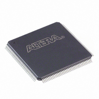
EP2C8T144I8N Altera, EP2C8T144I8N Datasheet - Page 97

EP2C8T144I8N
Manufacturer Part Number
EP2C8T144I8N
Description
IC CYCLONE II FPGA 8K 144-TQFP
Manufacturer
Altera
Series
Cyclone® IIr
Datasheet
1.EP2C5T144C8N.pdf
(168 pages)
Specifications of EP2C8T144I8N
Number Of Logic Elements/cells
8256
Number Of Labs/clbs
516
Total Ram Bits
165888
Number Of I /o
85
Voltage - Supply
1.15 V ~ 1.25 V
Mounting Type
Surface Mount
Operating Temperature
-40°C ~ 100°C
Package / Case
144-TQFP, 144-VQFP
Family Name
Cyclone® II
Number Of Logic Blocks/elements
8256
# I/os (max)
85
Frequency (max)
402.58MHz
Process Technology
90nm
Operating Supply Voltage (typ)
1.2V
Logic Cells
8256
Ram Bits
165888
Operating Supply Voltage (min)
1.15V
Operating Supply Voltage (max)
1.25V
Operating Temp Range
-40C to 100C
Operating Temperature Classification
Industrial
Mounting
Surface Mount
Pin Count
144
Package Type
TQFP
Lead Free Status / RoHS Status
Lead free / RoHS Compliant
Number Of Gates
-
Lead Free Status / Rohs Status
Compliant
Other names
544-2157
Available stocks
Company
Part Number
Manufacturer
Quantity
Price
Company:
Part Number:
EP2C8T144I8N
Manufacturer:
ALTERA31
Quantity:
387
Part Number:
EP2C8T144I8N
Manufacturer:
ALTERA/阿尔特拉
Quantity:
20 000
Altera Corporation
February 2008
Notes to
(1)
(2)
1.5-V HSTL class I
1.5V HSTL class II
Table 5–7. DC Characteristics of User I/O Pins Using Single-Ended Standards
I/O Standard
The values in this table are based on the conditions listed in
This specification is supported across all the programmable drive settings available as shown in the
Architecture
Table
5–7:
chapter of the Cyclone II Device Handbook.
I
OL
16
(mA)
Differential I/O Standards
The RSDS and mini-LVDS I/O standards are only supported on output
pins. The LVDS I/O standard is supported on both receiver input pins
and transmitter output pins.
1
Figure 5–1
standards (LVDS, LVPECL, differential 1.5-V HSTL class I and II,
differential 1.8-V HSTL class I and II, differential SSTL-2 class I and II, and
differential SSTL-18 class I and II).
8
Test Conditions
For more information on how these differential I/O standards
are implemented, refer to the
Cyclone II Devices
shows the receiver input waveforms for all differential I/O
I
OH
–16
–8
(mA)
chapter of the Cyclone II Device Handbook.
Tables 5–2
Maximum V
DC Characteristics and Timing Specifications
0.4
0.4
Cyclone II Device Handbook, Volume 1
and 5–6.
High-Speed Differential Interfaces in
Voltage Thresholds
OL
(V)
Notes
(1),
Minimum V
V
V
(2)
C C I O
C C I O
(Part 2 of 2)
Cyclone II
– 0.4
– 0.4
OH
(V)
5–7


