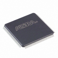
EP2C8T144I8N Altera, EP2C8T144I8N Datasheet - Page 13

EP2C8T144I8N
Manufacturer Part Number
EP2C8T144I8N
Description
IC CYCLONE II FPGA 8K 144-TQFP
Manufacturer
Altera
Series
Cyclone® IIr
Datasheet
1.EP2C5T144C8N.pdf
(168 pages)
Specifications of EP2C8T144I8N
Number Of Logic Elements/cells
8256
Number Of Labs/clbs
516
Total Ram Bits
165888
Number Of I /o
85
Voltage - Supply
1.15 V ~ 1.25 V
Mounting Type
Surface Mount
Operating Temperature
-40°C ~ 100°C
Package / Case
144-TQFP, 144-VQFP
Family Name
Cyclone® II
Number Of Logic Blocks/elements
8256
# I/os (max)
85
Frequency (max)
402.58MHz
Process Technology
90nm
Operating Supply Voltage (typ)
1.2V
Logic Cells
8256
Ram Bits
165888
Operating Supply Voltage (min)
1.15V
Operating Supply Voltage (max)
1.25V
Operating Temp Range
-40C to 100C
Operating Temperature Classification
Industrial
Mounting
Surface Mount
Pin Count
144
Package Type
TQFP
Lead Free Status / RoHS Status
Lead free / RoHS Compliant
Number Of Gates
-
Lead Free Status / Rohs Status
Compliant
Other names
544-2157
Available stocks
Company
Part Number
Manufacturer
Quantity
Price
Company:
Part Number:
EP2C8T144I8N
Manufacturer:
ALTERA31
Quantity:
387
Part Number:
EP2C8T144I8N
Manufacturer:
ALTERA/阿尔特拉
Quantity:
20 000
Functional
Description
Altera Corporation
February 2007
CII51002-3.1
Cyclone
architecture to implement custom logic. Column and row interconnects
of varying speeds provide signal interconnects between logic array
blocks (LABs), embedded memory blocks, and embedded multipliers.
The logic array consists of LABs, with 16 logic elements (LEs) in each
LAB. An LE is a small unit of logic providing efficient implementation of
user logic functions. LABs are grouped into rows and columns across the
device. Cyclone II devices range in density from 4,608 to 68,416 LEs.
Cyclone II devices provide a global clock network and up to four
phase-locked loops (PLLs). The global clock network consists of up to 16
global clock lines that drive throughout the entire device. The global clock
network can provide clocks for all resources within the device, such as
input/output elements (IOEs), LEs, embedded multipliers, and
embedded memory blocks. The global clock lines can also be used for
other high fan-out signals. Cyclone II PLLs provide general-purpose
clocking with clock synthesis and phase shifting as well as external
outputs for high-speed differential I/O support.
M4K memory blocks are true dual-port memory blocks with 4K bits of
memory plus parity (4,608 bits). These blocks provide dedicated true
dual-port, simple dual-port, or single-port memory up to 36-bits wide at
up to 260 MHz. These blocks are arranged in columns across the device
in between certain LABs. Cyclone II devices offer between 119 to
1,152 Kbits of embedded memory.
Each embedded multiplier block can implement up to either two 9 × 9-bit
multipliers, or one 18 × 18-bit multiplier with up to 250-MHz
performance. Embedded multipliers are arranged in columns across the
device.
Each Cyclone II device I/O pin is fed by an IOE located at the ends of LAB
rows and columns around the periphery of the device. I/O pins support
various single-ended and differential I/O standards, such as the 66- and
33-MHz, 64- and 32-bit PCI standard, PCI-X, and the LVDS I/O standard
at a maximum data rate of 805 megabits per second (Mbps) for inputs and
640 Mbps for outputs. Each IOE contains a bidirectional I/O buffer and
three registers for registering input, output, and output-enable signals.
Dual-purpose DQS, DQ, and DM pins along with delay chains (used to
®
II devices contain a two-dimensional row- and column-based
2. Cyclone II Architecture
2–1


