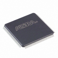
EP2C8T144I8N Altera, EP2C8T144I8N Datasheet - Page 49

EP2C8T144I8N
Manufacturer Part Number
EP2C8T144I8N
Description
IC CYCLONE II FPGA 8K 144-TQFP
Manufacturer
Altera
Series
Cyclone® IIr
Datasheet
1.EP2C5T144C8N.pdf
(168 pages)
Specifications of EP2C8T144I8N
Number Of Logic Elements/cells
8256
Number Of Labs/clbs
516
Total Ram Bits
165888
Number Of I /o
85
Voltage - Supply
1.15 V ~ 1.25 V
Mounting Type
Surface Mount
Operating Temperature
-40°C ~ 100°C
Package / Case
144-TQFP, 144-VQFP
Family Name
Cyclone® II
Number Of Logic Blocks/elements
8256
# I/os (max)
85
Frequency (max)
402.58MHz
Process Technology
90nm
Operating Supply Voltage (typ)
1.2V
Logic Cells
8256
Ram Bits
165888
Operating Supply Voltage (min)
1.15V
Operating Supply Voltage (max)
1.25V
Operating Temp Range
-40C to 100C
Operating Temperature Classification
Industrial
Mounting
Surface Mount
Pin Count
144
Package Type
TQFP
Lead Free Status / RoHS Status
Lead free / RoHS Compliant
Number Of Gates
-
Lead Free Status / Rohs Status
Compliant
Other names
544-2157
Available stocks
Company
Part Number
Manufacturer
Quantity
Price
Company:
Part Number:
EP2C8T144I8N
Manufacturer:
ALTERA31
Quantity:
387
Part Number:
EP2C8T144I8N
Manufacturer:
ALTERA/阿尔特拉
Quantity:
20 000
I/O Structure &
Features
Altera Corporation
February 2007
f
There are five dynamic control input signals that feed the embedded
multiplier: signa, signb, clk, clkena, and aclr. signa and signb
can be registered to match the data signal input path. The same clk,
clkena, and aclr signals feed all registers within a single embedded
multiplier.
For more information on Cyclone II embedded multipliers, see the
Embedded Multipliers in Cyclone II Devices chapter.
IOEs support many features, including:
■
■
■
■
■
■
■
■
■
■
■
■
Cyclone II device IOEs contain a bidirectional I/O buffer and three
registers for complete embedded bidirectional single data rate transfer.
Figure 2–20
input register, one output register, and one output enable register. You can
use the input registers for fast setup times and output registers for fast
clock-to-output times. Additionally, you can use the output enable (OE)
register for fast clock-to-output enable timing. The Quartus II software
automatically duplicates a single OE register that controls multiple
output or bidirectional pins. You can use IOEs as input, output, or
bidirectional pins.
Differential and single-ended I/O standards
3.3-V, 64- and 32-bit, 66- and 33-MHz PCI compliance
Joint Test Action Group (JTAG) boundary-scan test (BST) support
Output drive strength control
Weak pull-up resistors during configuration
Tri-state buffers
Bus-hold circuitry
Programmable pull-up resistors in user mode
Programmable input and output delays
Open-drain outputs
DQ and DQS I/O pins
V
REF
pins
shows the Cyclone II IOE structure. The IOE contains one
Cyclone II Device Handbook, Volume 1
Cyclone II Architecture
2–37


