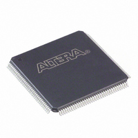
EP2C8T144I8N Altera, EP2C8T144I8N Datasheet - Page 21

EP2C8T144I8N
Manufacturer Part Number
EP2C8T144I8N
Description
IC CYCLONE II FPGA 8K 144-TQFP
Manufacturer
Altera
Series
Cyclone® IIr
Datasheet
1.EP2C5T144C8N.pdf
(168 pages)
Specifications of EP2C8T144I8N
Number Of Logic Elements/cells
8256
Number Of Labs/clbs
516
Total Ram Bits
165888
Number Of I /o
85
Voltage - Supply
1.15 V ~ 1.25 V
Mounting Type
Surface Mount
Operating Temperature
-40°C ~ 100°C
Package / Case
144-TQFP, 144-VQFP
Family Name
Cyclone® II
Number Of Logic Blocks/elements
8256
# I/os (max)
85
Frequency (max)
402.58MHz
Process Technology
90nm
Operating Supply Voltage (typ)
1.2V
Logic Cells
8256
Ram Bits
165888
Operating Supply Voltage (min)
1.15V
Operating Supply Voltage (max)
1.25V
Operating Temp Range
-40C to 100C
Operating Temperature Classification
Industrial
Mounting
Surface Mount
Pin Count
144
Package Type
TQFP
Lead Free Status / RoHS Status
Lead free / RoHS Compliant
Number Of Gates
-
Lead Free Status / Rohs Status
Compliant
Other names
544-2157
Available stocks
Company
Part Number
Manufacturer
Quantity
Price
Company:
Part Number:
EP2C8T144I8N
Manufacturer:
ALTERA31
Quantity:
387
Part Number:
EP2C8T144I8N
Manufacturer:
ALTERA/阿尔特拉
Quantity:
20 000
Figure 2–7. LAB-Wide Control Signals
Altera Corporation
February 2007
Dedicated
LAB Row
Clocks
Local
Interconnect
Local
Interconnect
Local
Interconnect
Local
Interconnect
This gives a maximum of seven control signals at a time. When using the
LAB-wide synchronous load, the clkena of labclk1 is not available.
Additionally, register packing and synchronous load cannot be used
simultaneously.
Each LAB can have up to four non-global control signals. Additional LAB
control signals can be used as long as they are global signals.
Synchronous clear and load signals are useful for implementing counters
and other functions. The synchronous clear and synchronous load signals
are LAB-wide signals that affect all registers in the LAB.
Each LAB can use two clocks and two clock enable signals. Each LAB’s
clock and clock enable signals are linked. For example, any LE in a
particular LAB using the labclk1 signal also uses labclkena1. If the
LAB uses both the rising and falling edges of a clock, it also uses both
LAB-wide clock signals. De-asserting the clock enable signal turns off the
LAB-wide clock.
The LAB row clocks [5..0] and LAB local interconnect generate the LAB-
wide control signals. The MultiTrack
allows clock and control signal distribution in addition to data.
shows the LAB control signal generation circuit.
LAB-wide signals control the logic for the register’s clear signal. The LE
directly supports an asynchronous clear function. Each LAB supports up
to two asynchronous clear signals (labclr1 and labclr2).
6
labclk1
labclkena1
labclk2
labclkena2
Cyclone II Device Handbook, Volume 1
™
syncload
interconnect’s inherent low skew
labclr1
Cyclone II Architecture
labclr2
Figure 2–7
synclr
2–9


