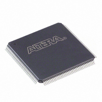
EP2C8T144I8N Altera, EP2C8T144I8N Datasheet - Page 100

EP2C8T144I8N
Manufacturer Part Number
EP2C8T144I8N
Description
IC CYCLONE II FPGA 8K 144-TQFP
Manufacturer
Altera
Series
Cyclone® IIr
Datasheet
1.EP2C5T144C8N.pdf
(168 pages)
Specifications of EP2C8T144I8N
Number Of Logic Elements/cells
8256
Number Of Labs/clbs
516
Total Ram Bits
165888
Number Of I /o
85
Voltage - Supply
1.15 V ~ 1.25 V
Mounting Type
Surface Mount
Operating Temperature
-40°C ~ 100°C
Package / Case
144-TQFP, 144-VQFP
Family Name
Cyclone® II
Number Of Logic Blocks/elements
8256
# I/os (max)
85
Frequency (max)
402.58MHz
Process Technology
90nm
Operating Supply Voltage (typ)
1.2V
Logic Cells
8256
Ram Bits
165888
Operating Supply Voltage (min)
1.15V
Operating Supply Voltage (max)
1.25V
Operating Temp Range
-40C to 100C
Operating Temperature Classification
Industrial
Mounting
Surface Mount
Pin Count
144
Package Type
TQFP
Lead Free Status / RoHS Status
Lead free / RoHS Compliant
Number Of Gates
-
Lead Free Status / Rohs Status
Compliant
Other names
544-2157
Available stocks
Company
Part Number
Manufacturer
Quantity
Price
Company:
Part Number:
EP2C8T144I8N
Manufacturer:
ALTERA31
Quantity:
387
Part Number:
EP2C8T144I8N
Manufacturer:
ALTERA/阿尔特拉
Quantity:
20 000
Operating Conditions
Figure 5–2. Transmitter Output Waveforms for Differential I/O Standards
Notes to
(1)
(2)
(3)
5–10
Cyclone II Device Handbook, Volume 1
LVDS
mini-LVDS
RSDS
Differential 1.5-V
HSTL class I
and II
Table 5–9. DC Characteristics for User I/O Pins Using Differential I/O Standards
I/O Standard
V
V
The p – n waveform is a function of the positive channel (p) and the negative channel (n).
OD
OCM
(3)
(2)
Figure
is the output differential voltage. V
is the output common mode voltage. V
Single-Ended Waveform
Differential Waveform (Mathematical Function of Positive and Negative Channel)
(2)
5–2:
Min
250
300
100
—
V
OD
V
Typ
—
—
—
—
OCM
(mV)
Figure 5–2
differential output standards (LVDS, mini-LVDS, RSDS, differential 1.5-V
HSTL class I and II, differential 1.8-V HSTL class I and II, differential
SSTL-2 class I and II, and differential SSTL-18 class I and II).
Table 5–9
I/O standards.
(2)
V
OD
Max
600
600
600
—
(1)
shows the DC characteristics for user I/O pins with differential
OD
shows the transmitter output waveforms for all supported
ΔV
Min Max
—
—
—
—
= |p – n|.
V
OD
OD
OCM
(mV)
(1)
50
50
—
—
= (p + n)/2.
1.125
1.125
1.125
Min
—
V
OCM
1.25
1.25
1.25
Typ
—
(V)
V
OD
1.375
1.375
1.375
Max
—
(1)
0 V
p − n (3)
Positive Channel (p) = V
Negative Channel (n) = V
Ground
V
– 0.4
Min
C C I O
—
—
—
V
Note (1)
OH
(V)
Max
—
—
—
—
Altera Corporation
(Part 1 of 2)
February 2008
OH
Min
OL
—
—
—
—
V
OL
(V)
Max
0.4
—
—
—


