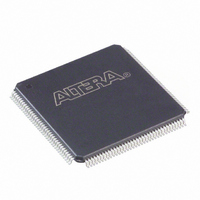
EP2C8T144I8N Altera, EP2C8T144I8N Datasheet - Page 162

EP2C8T144I8N
Manufacturer Part Number
EP2C8T144I8N
Description
IC CYCLONE II FPGA 8K 144-TQFP
Manufacturer
Altera
Series
Cyclone® IIr
Datasheet
1.EP2C5T144C8N.pdf
(168 pages)
Specifications of EP2C8T144I8N
Number Of Logic Elements/cells
8256
Number Of Labs/clbs
516
Total Ram Bits
165888
Number Of I /o
85
Voltage - Supply
1.15 V ~ 1.25 V
Mounting Type
Surface Mount
Operating Temperature
-40°C ~ 100°C
Package / Case
144-TQFP, 144-VQFP
Family Name
Cyclone® II
Number Of Logic Blocks/elements
8256
# I/os (max)
85
Frequency (max)
402.58MHz
Process Technology
90nm
Operating Supply Voltage (typ)
1.2V
Logic Cells
8256
Ram Bits
165888
Operating Supply Voltage (min)
1.15V
Operating Supply Voltage (max)
1.25V
Operating Temp Range
-40C to 100C
Operating Temperature Classification
Industrial
Mounting
Surface Mount
Pin Count
144
Package Type
TQFP
Lead Free Status / RoHS Status
Lead free / RoHS Compliant
Number Of Gates
-
Lead Free Status / Rohs Status
Compliant
Other names
544-2157
Available stocks
Company
Part Number
Manufacturer
Quantity
Price
Company:
Part Number:
EP2C8T144I8N
Manufacturer:
ALTERA31
Quantity:
387
Part Number:
EP2C8T144I8N
Manufacturer:
ALTERA/阿尔特拉
Quantity:
20 000
Duty Cycle Distortion
5–72
Cyclone II Device Handbook, Volume 1
For DDIO outputs, you can calculate actual half period from the
following equation:
For example, if the DDR output I/O standard is SSTL-2 Class II, the
maximum DCD for a –5 device is 155 ps (refer to
frequency is 167 MHz, the half-clock period T/2 is:
Notes to
(1)
(2)
1.5-V
SSTL-2 Class I
SSTL-2 Class II
SSTL-18 Class I
HSTL-18 Class I
HSTL-15 Class I
Differential SSTL-2 Class I
Differential SSTL-2 Class II
Differential SSTL-18 Class I
Differential HSTL-18 Class I
Differential HSTL-15 Class I
LVDS
Simple RSDS
Mini LVDS
PCI
PCI-X
Table 5–57. Maximum for DDIO Output on Row Pins with PLL in the Clock
Path
Row Pins with PLL in the Clock Path
Actual half period = ideal half period – maximum DCD
T/2 = 1/(2* f )= 1 /(2*167 MHz) = 3 ns = 3000 ps
The DCD specification is characterized using the maximum drive strength
available for each I/O standard.
Numbers are applicable for commercial, industrial, and automotive devices.
Notes
Table
(1),
5–57:
(2)
(Part 2 of 2)
280
150
155
180
180
205
150
155
180
180
205
100
285
285
C6
95
95
280
190
200
240
235
220
190
200
240
235
220
110
155
110
305
305
Table
C7
Altera Corporation
5–57). If the clock
280
230
230
260
235
220
230
230
260
235
220
120
155
120
335
335
C8
February 2008
Unit
ps
ps
ps
ps
ps
ps
ps
ps
ps
ps
ps
ps
ps
ps
ps
ps


