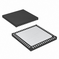
MAX19711ETN+T Maxim Integrated Products, MAX19711ETN+T Datasheet - Page 31

MAX19711ETN+T
Manufacturer Part Number
MAX19711ETN+T
Description
IC ANLG FRNT END 56-TQFN
Manufacturer
Maxim Integrated Products
Datasheet
1.MAX19711ETN.pdf
(36 pages)
Specifications of MAX19711ETN+T
Number Of Bits
10
Number Of Channels
2
Power (watts)
37.5mW
Voltage - Supply, Analog
3V
Voltage - Supply, Digital
3V
Package / Case
56-TQFN Exposed Pad
Lead Free Status / RoHS Status
Lead free / RoHS Compliant
70kΩ. If single-ended outputs are desired, use an
amplifier to provide differential-to-single-ended conver-
sion and select an amplifier with proper input common-
mode voltage range.
Figure 14 illustrates a typical CDMA application circuit.
The MAX19711 is designed to interface directly with the
MAX2504 and MAX2584 radio front-ends to provide
a complete “RF-to-Bits” front-end solution. The
MAX19711 provides several features that allow direct
interface to the MAX2584 and MAX2504:
•
•
•
•
•
Figure 13. Rx ADC DC-Coupled Differential Drive
Integrated Tx filters reduce component count, lower
cost, and meet CDMA spectral mask requirements
Programmable DC common-mode Tx output levels
eliminate discrete DC-level-shifting components
while preserving Tx DAC full dynamic range
Optimized Tx full-scale output level eliminates dis-
crete amplifiers for ID–QD gain control
Tx-ID–QD offset correction eliminates discrete trim
DACs for offset trim to improve sideband/carrier
suppression
1µs settling time aux-DACs for VGA and AGC control
allow fast, accurate Tx power and Rx gain control
______________________________________________________________________________________
CDMA Application
R1
600Ω
R2
600Ω
R3
600Ω
600Ω
600Ω
600Ω
600Ω
R10
R8
R4
R6
10-Bit, 11Msps, Full-Duplex
600Ω
600Ω
600Ω
600Ω
R11
R9
R7
R5
The MAX19711 requires high-speed board layout design
techniques. Refer to the MAX19711 EV kit data sheet for a
board layout reference. Place all bypass capacitors as
close to the device as possible, preferably on the same
side of the board as the device, using surface-mount
devices for minimum inductance. Bypass V
with a 0.1µF ceramic capacitor in parallel with a 2.2µF
capacitor. Bypass OV
capacitor in parallel with a 2.2µF capacitor. Bypass REFP,
REFN, and COM each to GND with a 0.33µF ceramic
capacitor. Bypass REFIN to GND with a 0.1µF capacitor.
Multilayer boards with separated ground and power
planes yield the highest level of signal integrity. Use a
split ground plane arranged to match the physical loca-
tion of the analog ground (GND) and the digital output-
driver ground (OGND) on the device package. Connect
the MAX19711 exposed backside paddle to the GND
plane. Join the two ground planes at a single point so
the noisy digital ground currents do not interfere with
the analog ground plane. The ideal location for this
connection can be determined experimentally at a
point along the gap between the two ground planes.
Make this connection with a low-value, surface-mount
resistor (1Ω to 5Ω), a ferrite bead, or a direct short.
22Ω
R
22Ω
R
ISO
ISO
Grounding, Bypassing, and
Analog Front-End
C
5pF
C
5pF
IN
IN
IAP
IAN
COM
DD
to OGND with a 0.1µF ceramic
MAX19711
Board Layout
DD
to GND
31


