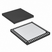
MAX19711ETN+T Maxim Integrated Products, MAX19711ETN+T Datasheet - Page 15

MAX19711ETN+T
Manufacturer Part Number
MAX19711ETN+T
Description
IC ANLG FRNT END 56-TQFN
Manufacturer
Maxim Integrated Products
Datasheet
1.MAX19711ETN.pdf
(36 pages)
Specifications of MAX19711ETN+T
Number Of Bits
10
Number Of Channels
2
Power (watts)
37.5mW
Voltage - Supply, Analog
3V
Voltage - Supply, Digital
3V
Package / Case
56-TQFN Exposed Pad
Lead Free Status / RoHS Status
Lead free / RoHS Compliant
The MAX19711 integrates a dual, 10-bit Rx ADC and a
dual, 10-bit Tx DAC with CDMA baseband filters while
providing ultra-low power and high dynamic perfor-
mance at 11Msps conversion rate. The Rx ADC analog
5, 7, 12, 40, 50
2, 8, 11, 39,
41, 47, 51
13–22
25–34
PIN
10
23
24
35
36
37
38
42
43
44
45
46
48
49
52
53
54
55
56
—
1
3
4
6
9
AD0–AD9
DA0–DA9
CS/WAKE
OGND
______________________________________________________________________________________
NAME
DOUT
REFIN
OV
ADC2
ADC1
DAC3
DAC2
DAC1
REFP
SCLK
REFN
COM
GND
QAN
QDN
QAP
QDP
CLK
V
IAN
DIN
IDN
IDP
IAP
EP
DD
DD
Detailed Description
Positive Reference Voltage Input Terminal. Bypass with a 0.33µF capacitor to GND as close to REFP
as possible.
Analog Supply Voltage. Bypass V
a 0.1µF capacitor.
Channel-IA Positive Analog Input. For single-ended operation, connect signal source to IAP.
Channel-IA Negative Analog Input. For single-ended operation, connect IAN to COM.
Analog Ground. Connect all GND pins to ground plane.
Conversion Clock Input. Clock signal for both receive ADCs and transmit DACs.
Channel-QA Negative Analog Input. For single-ended operation, connect QAN to COM.
Channel-QA Positive Analog Input. For single-ended operation, connect signal source to QAP.
Receive ADC Digital Outputs. AD9 is the most significant bit (MSB) and AD0 is the least significant
bit (LSB).
Output-Driver Ground
Output-Driver Power Supply. Supply range from +1.8V to V
combination of a 2.2µF capacitor in parallel with a 0.1µF capacitor.
Transmit DAC Digital Inputs. DA9 is the most significant bit (MSB) and DA0 is the least significant bit
(LSB). DA0–DA9 are internally pulled up to OV
Aux-ADC Digital Output
3-Wire Serial-Interface Data Input. Data is latched on the rising edge of SCLK.
3-Wire Serial-Interface Clock Input
3-Wire Serial-Interface Chip-Select/WAKE Input. When the MAX19711 is in shutdown, CS/WAKE
controls the wake-up function. See the Wake-Up Function section.
Selectable Auxiliary ADC Analog Input 2
Selectable Auxiliary ADC Analog Input 1
Auxiliary DAC3 Analog Output (V
Auxiliary DAC2 Analog Output (V
Auxiliary DAC1 Analog Output (AFC DAC, V
Tx Path Channel-ID Differential Negative Output
Tx Path Channel-ID Differential Positive Output
Tx Path Channel-QD Differential Negative Output
Tx Path Channel-QD Differential Positive Output
Reference Input. Connect to V
Common-Mode Voltage I/O. Bypass COM to GND with a 0.33µF capacitor.
Negative Reference Voltage Input Terminal. Rx ADC conversion range is ±(V
REFN to GND with a 0.33µF capacitor.
Exposed Paddle. Exposed paddle is internally connected to GND. Connect EP to the GND plane.
10-Bit, 11Msps, Full-Duplex
DD
OUT
OUT
DD
for internal reference.
to GND with a combination of a 2.2µF capacitor in parallel with
= 0 at Power-Up)
= 0 at Power-Up)
input amplifiers are fully differential and accept
1.024V
puts are fully differential with selectable ±410mV or
±500mV full-scale output, selectable common-mode
DC level, and adjustable channel ID–QD offset trim.
OUT
FUNCTION
P-P
DD.
= 1.1V at Power-Up)
full-scale signals. The Tx DAC analog out-
Analog Front-End
DD
. Bypass OV
Pin Description
DD
REFP
to OGND with a
- V
REFN
). Bypass
15


