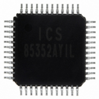
ICS85352AYILF IDT, Integrated Device Technology Inc, ICS85352AYILF Datasheet

ICS85352AYILF
Specifications of ICS85352AYILF
85352AYILF
Available stocks
Related parts for ICS85352AYILF
ICS85352AYILF Summary of contents
Page 1
Bit, 2-to-1, 3.3V, 2.5V LVPECL Clock Buffer General Description The ICS85352I bit, 2-to-1 LVPECL Clock Buffer. Individual input select controls support independent multiplexer operation from a common clock input source. Clock inputs accept most standard differential ...
Page 2
ICS85352I Data Sheet Table 1. Pin Descriptions Number Name 1, 2 Q0, nQ0 3, 4 Q1, nQ1 5, 6 Q2, nQ2 7, 8 Q3, nQ3 9, 10 Q4, nQ4 11, 12 Q5, nQ5 25, 26 nQ11, Q11 27, 28 nQ10, ...
Page 3
ICS85352I Data Sheet Absolute Maximum Ratings NOTE: Stresses beyond those listed under Absolute Maximum Ratings may cause permanent damage to the device. These ratings are stress specifications only. Functional operation of product at these conditions or any conditions beyond those ...
Page 4
ICS85352I Data Sheet Table 4D. LVPECL DC Characteristics, V Symbol Parameter V Output High Voltage; NOTE Output Low Voltage; NOTE Peak-to-Peak Output Voltage Swing SWING NOTE 1: Outputs terminated with 50Ω ...
Page 5
ICS85352I Data Sheet Additive Phase Jitter The spectral purity in a band at a specific offset from the fundamental compared to the power of the fundamental is called the dBc Phase Noise. This value is normally expressed using a Phase ...
Page 6
ICS85352I Data Sheet Parameter Measurement Information 2V V CC, V CCO LVPECL V EE -1.3V ± -0.165V 3.3V Core/ 3.3V LVPECL Output Load AC Test Circuit V CC nCLK[0:1] V Cross Points PP CLK[0: Differential Input Level nQx ...
Page 7
ICS85352I Data Sheet Parameter Measurement Information, continued nQ[0:11] Q[0:11 PERIOD t odc = t PERIOD Output Duty Cycle/Pulse Width/Period Application Information Recommendations for Unused Input and Output Pins Inputs: LVCMOS Control Pins All control pins have internal ...
Page 8
ICS85352I Data Sheet Wiring the Differential Input to Accept Single-Ended Levels Figure 1 shows how a differential input can be wired to accept single ended levels. The reference voltage V the bias resistors R1 and R2. The bypass capacitor (C1) ...
Page 9
ICS85352I Data Sheet EPAD Thermal Release Path In order to maximize both the removal of heat from the package and the electrical performance, a land pattern must be incorporated on the Printed Circuit Board (PCB) within the footprint of the ...
Page 10
ICS85352I Data Sheet Differential Clock Input Interface The CLK /nCLK accepts LVDS, LVPECL, LVHSTL, SSTL, HCSL and other differential signals. Both V and V SWING V input requirements. Figures show interface examples CMR for the CLK/nCLK input ...
Page 11
ICS85352I Data Sheet Termination for 3.3V LVPECL Outputs The clock layout topology shown below is a typical termination for LVPECL outputs. The two different layouts mentioned are recommended only as guidelines. The differential outputs are low impedance follower outputs that ...
Page 12
ICS85352I Data Sheet Termination for 2.5V LVPECL Outputs Figure 5A and Figure 5B show examples of termination for 2.5V LVPECL driver. These terminations are equivalent to terminating 50Ω – 2V. For V = 2.5V, the V CC CCO ...
Page 13
ICS85352I Data Sheet Application Schematic Example Figure 6 shows an example of ICS85352I application schematic. In this example, the device is operated at V capacitor should be located as close as possible to the power pin. For CLK1 nCLK1 SEL8 ...
Page 14
ICS85352I Data Sheet Power Considerations This section provides information on power dissipation and junction temperature for the ICS85352I. Equations and example calculations are also provided. 1. Power Dissipation. The total power dissipation for the ICS85352I is the sum of the ...
Page 15
ICS85352I Data Sheet 3. Calculations and Equations. The purpose of this section is to calculate the power dissipation for the LVPECL output pairs. LVPECL output driver circuit and termination are shown in Figure 5. V CCO Q1 Figure 5. LVPECL ...
Page 16
ICS85352I Data Sheet Reliability Information θ Table 7. vs. Air Flow Table for a 48 Lead TQFP, E-Pad JA Linear Feet per Minute Multi-Layer PCB, JEDEC Standard Test Boards Transistor Count The transistor count for ICS85352I is: 2252 ICS85352AYI REVISION ...
Page 17
ICS85352I Data Sheet Package Outline and Package Dimensions Package Outline - Y Suffix for 48 Lead TQFP, E-Pad Table 8. Package Dimensions 48 Lead TQFP, E-Pad JEDEC Variation: ABC - HD All Dimensions in Millimeters Symbol Minimum Nominal N 48 ...
Page 18
ICS85352I Data Sheet Table 9. Ordering Information Part/Order Number Marking 85352AYI ICS85352AYI 85352AYIT ICS85352AYI 85352AYILF ICS85352AYIL 85352AYILFT ICS85352AYIL NOTE: Parts that are ordered with an "LF" suffix to the part number are the Pb-Free configuration and are RoHS compliant. While ...
Page 19
ICS85352I Data Sheet Revision History Sheet Rev Table Page Description of Change 1 Features Section - added lead-free bullet. 6 Added Recommendations for Unused Input and Output Pins Added Thermal Release Path Ordering Information Table - ...
Page 20
ICS85352I Data Sheet We’ve Got Your Timing Solution 6024 Silver Creek Valley Road Sales 800-345-7015 (inside USA) San Jose, California 95138 +408-284-8200 (outside USA) Fax: 408-284-2775 www.IDT.com/go/contactIDT DISCLAIMER Integrated Device Technology, Inc. (IDT) and its subsidiaries reserve the right to ...


