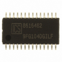
ICS9FG104DGILFT IDT, Integrated Device Technology Inc, ICS9FG104DGILFT Datasheet

ICS9FG104DGILFT
Specifications of ICS9FG104DGILFT
9FG104DGILFT
Related parts for ICS9FG104DGILFT
ICS9FG104DGILFT Summary of contents
Page 1
Frequency Generator for CPU, QPI, FBD, PCIe Gen 2 & SATA Description The ICS9FG104D is a Frequency Timing Generator that provides 4 differential output pairs that are compliant to the Intel CK410 specification. It also provides support for PCI-Express and ...
Page 2
ICS9FG104D Frequency Generator for CPU, QPI, FBD, PCIe Gen 2 & SATA Pin Configuration XIN/CLKIN VDD 3 GND 4 REFOUT 5 vFS2 6 DIF_3 7 DIF_3# 8 VDD 9 GND 10 DIF_2 11 DIF_2# 12 SDATA 13 ...
Page 3
ICS9FG104D Frequency Generator for CPU, QPI, FBD, PCIe Gen 2 & SATA Pin Description PIN # PIN NAME 1 XIN/CLKIN VDD 4 GND 5 REFOUT 6 vFS2 7 DIF_3 8 DIF_3# 9 VDD 10 GND 11 DIF_2 ...
Page 4
ICS9FG104D Frequency Generator for CPU, QPI, FBD, PCIe Gen 2 & SATA Absolute Max Symbol Parameter VDDxx 3.3V Supply Voltage Ts Storage Temperature Tambient Ambient Operating Temp•(Commerical Grade) Tambient Ambient Operating Temp•(Industrial Grade) Tcase Case Temperature ESD prot Input ESD ...
Page 5
ICS9FG104D Frequency Generator for CPU, QPI, FBD, PCIe Gen 2 & SATA Electrical Characteristics - DIF 0.7V Current Mode Differential Pair 3.3 V +/-5 IENT A DD PARAMETER SYMBOL Output ...
Page 6
ICS9FG104D Frequency Generator for CPU, QPI, FBD, PCIe Gen 2 & SATA Electrical Characteristics - REF-14.318/25 MHz 3.3 V +/-5%; IENT A DD PARAMETER SYMBOL Long Accuracy ppm Clock period T ...
Page 7
ICS9FG104D Frequency Generator for CPU, QPI, FBD, PCIe Gen 2 & SATA General SMBus serial interface information for the ICS9FG104D How to Write: • Controller (host) sends a start bit. • Controller (host) sends the write address DC • ICS ...
Page 8
ICS9FG104D Frequency Generator for CPU, QPI, FBD, PCIe Gen 2 & SATA SMBus Table: Device Control Register, READ/WRITE ADDRESS (DC/DD) Byte 0 Pin # Name 17 Bit 7 6 Bit 6 24 Bit 5 25 Bit 4 16 Bit 3 ...
Page 9
ICS9FG104D Frequency Generator for CPU, QPI, FBD, PCIe Gen 2 & SATA SMBus Table: Frequency Select Readback Register Byte 3 Pin # Name SEL14M_25M# 27 Bit 7 (FS3) 6 FS2 Bit 6 44 FS1 Bit 5 45 FS0 Bit 4 ...
Page 10
ICS9FG104D Frequency Generator for CPU, QPI, FBD, PCIe Gen 2 & SATA SMBus Table: Reserved Register Byte 7 Pin # Name - Bit 7 - Bit 6 - Bit 5 - Bit 4 - Bit 3 - Bit 2 - ...
Page 11
ICS9FG104D Frequency Generator for CPU, QPI, FBD, PCIe Gen 2 & SATA SMBus Table: PLL Frequency Control Register Byte 11 Pin # Name - PLL N Div7 Bit 7 - PLL N Div6 Bit 6 - PLL N Div5 Bit ...
Page 12
ICS9FG104D Frequency Generator for CPU, QPI, FBD, PCIe Gen 2 & SATA DIF_STOP# - Assertion (transition from '1' to '0') Asserting DIF_STOP# pin stops all DIF outputs that are set to be stoppable after their next transition. When the SMBus ...
Page 13
ICS9FG104D Frequency Generator for CPU, QPI, FBD, PCIe Gen 2 & SATA Common Recommendations for Differential Routing L1 length, route as non-coupled 50ohm trace L2 length, route as non-coupled 50ohm trace L3 length, route as non-coupled 50ohm trace Rs Rt ...
Page 14
ICS9FG104D Frequency Generator for CPU, QPI, FBD, PCIe Gen 2 & SATA Alternative Termination for LVDS and other Common Differential Signals (figure 3) Vdiff Vp-p Vcm 0.45v 0.22v 1.08 0.58 0.28 0.6 0.80 0.40 0.6 0.60 0.3 1.2 R1a = ...
Page 15
ICS9FG104D Frequency Generator for CPU, QPI, FBD, PCIe Gen 2 & SATA 28-Pin SSOP Package Drawing and Dimensions INDEX INDEX AREA AREA 45° Frequency Generator for CPU, QPI, ...
Page 16
ICS9FG104D Frequency Generator for CPU, QPI, FBD, PCIe Gen 2 & SATA 28-Pin TSSOP Package Drawing and Dimensions N E1 INDEX AREA Ordering Information Part/Order Number Shipping Packaging 9FG104DFLF 9FG104DFLFT Tape and Reel ...
Page 17
ICS9FG104D Frequency Generator for CPU, QPI, FBD, PCIe Gen 2 & SATA Revision History Rev. Issue Date Description 1. Created Rev D data sheet from original non revision specific version. 0.1 12/18/2008 2. Updated phase noise characterisitcs for Rev D. ...


