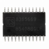
ICS85408BGLF IDT, Integrated Device Technology Inc, ICS85408BGLF Datasheet - Page 5

ICS85408BGLF
Manufacturer Part Number
ICS85408BGLF
Description
IC CLK DISTR DIFF-LVDS 24-TSSOP
Manufacturer
IDT, Integrated Device Technology Inc
Series
HiPerClockS™r
Type
Fanout Buffer (Distribution)r
Datasheet
1.ICS85408BGLF.pdf
(16 pages)
Specifications of ICS85408BGLF
Number Of Circuits
1
Ratio - Input:output
1:8
Differential - Input:output
Yes/Yes
Input
HCSL, LVDS, LVHSTL, LVPECL, SSTL
Output
LVDS
Frequency - Max
700MHz
Voltage - Supply
3.135 V ~ 3.465 V
Operating Temperature
0°C ~ 70°C
Mounting Type
Surface Mount
Package / Case
24-TSSOP
Frequency-max
700MHz
Number Of Outputs
16
Operating Supply Voltage (max)
3.465V
Operating Temp Range
0C to 70C
Propagation Delay Time
5ns
Operating Supply Voltage (min)
3.135V
Mounting
Surface Mount
Pin Count
24
Operating Supply Voltage (typ)
3.3V
Package Type
TSSOP
Duty Cycle
55%
Operating Temperature Classification
Commercial
Lead Free Status / RoHS Status
Lead free / RoHS Compliant
Other names
800-1182
800-1182-5
800-1182
85408BGLF
800-1182-5
800-1182
85408BGLF
Available stocks
Company
Part Number
Manufacturer
Quantity
Price
Part Number:
ICS85408BGLF
Manufacturer:
ICS
Quantity:
20 000
ICS85408 Datasheet
Table 4D. LVDS DC Characteristics, V
Table 5. AC Characteristics, V
NOTE: Electrical parameters are guaranteed over the specified ambient operating temperature range, which is established when the device is
mounted in a test socket with maintained transverse airflow greater than 500 lfpm. The device will meet specifications after thermal equilibrium
has been reached under these conditions.
NOTE: All parameters measured at f ≤ 622MHz unless noted otherwise.
NOTE 1: Measured from the differential input crossing point to the differential output crossing point.
NOTE 2: Defined as skew between outputs at the same supply voltage and with equal load conditions. Measured at the differential crossing
point of the input to the differential output crossing point.
NOTE 3: Defined as skew between outputs on different devices operating at the same supply voltages and with equal load conditions. Using
the same type of inputs on each device, the outputs are measured at the differential cross points.
NOTE 4: This parameter is defined in accordance with JEDEC Standard 65.
NOTE 5: These parameters are guaranteed by characterization. Not tested in production.
ICS85408BG REVISION B JUNE 25, 2009
Symbol
V
∆V
V
∆V
I
I
I
I
Symbol
f
t
tjit
tsk(o)
tsk(pp)
t
odc
t
t
Oz
OFF
OSD
OS
MAX
PD
R
PZL,
PLZ,
OD
OS
/ t
OD
OS
/I
OSB
F
t
t
PZH
PHZ
Parameter
Output Frequency
Propagation Delay; NOTE 1
Buffer Additive Phase Jitter, RMS;
refer to Additive Phase Jitter
Section
Output Skew; NOTE 2, 4
Part-to-Part Skew; NOTE 3, 4
Output Rise/Fall Time
Output Duty Cycle
Output Enable Time; NOTE 5
Output Disable Time; NOTE 5
Parameter
Differential Output Voltage
V
Offset Voltage
V
High Impedance Leakage
Power Off Leakage
Differential Output Short
Circuit Current
Output Short Circuit Current
OD
OS
Magnitude Change
Magnitude Change
DD
= 3.3V ± 5%, T
DD
= 3.3V ± 5%, T
Integration Range: (12kHz – 20MHz)
A
Test Conditions
= 0°C to 70°C
R
R
R
R
L
L
L
L
Test Conditions
= 100
= 100
= 100
= 100
156.25MHz,
20% to 80%
A
= 0°C to 70°C
Ω
Ω
Ω
Ω
5
LOW SKEW, 1-TO-8, DIFFERENTIAL-TO-LVDS CLOCK DISTRIBUTION CHIP
Minimum
1.125
250
-10
-1
Minimum
1.6
50
45
Typical
400
1.4
Typical
167
©2009 Integrated Device Technology, Inc.
Maximum
Maximum
600
+10
-5.5
1.6
-12
50
50
+1
700
550
600
2.4
50
55
5
5
Units
Units
mV
mV
mV
mA
mA
µA
µA
MHz
V
ps
ps
ps
ns
ns
ns
%
fs


