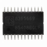
ICS85408BGLF IDT, Integrated Device Technology Inc, ICS85408BGLF Datasheet

ICS85408BGLF
Specifications of ICS85408BGLF
800-1182-5
800-1182
85408BGLF
Available stocks
Related parts for ICS85408BGLF
ICS85408BGLF Summary of contents
Page 1
Low Skew, 1-to-8, Differential-to-LVDS Clock General Description The ICS85408 is a low skew, high performance 1-to-8 ICS Differential-to-LVDS Clock Distribution Chip and a member of the HiPerClockS™ family of High HiPerClockS™ Performance Clock Solutions from IDT. The ICS85408 CLK, nCLK ...
Page 2
ICS85408 Datasheet Table 1. Pin Descriptions Number Name 1, 2 nQ6, Q6 Output 3, 4 nQ5, Q5 Output 5, 6 nQ4, Q4 Output 7, 8 nQ3, Q3 Output 9, 10 nQ2, Q2 Output 11, 12 nQ1, Q1 Output 13, 14 ...
Page 3
ICS85408 Datasheet Table 3B. Clock Input Function Table Inputs CLK nCLK Biased; NOTE 1 1 Biased; NOTE 1 Biased; NOTE 1 0 Biased; NOTE 1 1 NOTE 1: Please refer to the Application Information section, ...
Page 4
ICS85408 Datasheet Absolute Maximum Ratings NOTE: Stresses beyond those listed under Absolute Maximum Ratings may cause permanent damage to the device. These ratings are stress specifications only. Functional operation of product at these conditions or any conditions beyond those listed ...
Page 5
ICS85408 Datasheet Table 4D. LVDS DC Characteristics, V Symbol Parameter V Differential Output Voltage OD ∆V V Magnitude Change Offset Voltage OS ∆V V Magnitude Change High Impedance Leakage Oz I Power Off Leakage ...
Page 6
ICS85408 Datasheet Additive Phase Jitter The spectral purity in a band at a specific offset from the fundamental compared to the power of the fundamental is called the dBc Phase Noise. This value is normally expressed using a Phase noise ...
Page 7
ICS85408 Datasheet Parameter Measurement Information V DD 3.3V±5% POWER SUPPLY LVDS + Float GND – 3.3V LVDS Output Load AC Test Circuit nCLK CLK nQ[0:7] Q[0: Propagation Delay nQx Qx nQy Qy tsk(o) Output Skew ICS85408BG REVISION B ...
Page 8
ICS85408 Datasheet Parameter Measurement Information, continued nQ[0:7] 80% 20% Q[0: Output Rise/Fall Time V DD LVDS DC Input Differential Output Voltage Setup V DD LVDS DC Input Differential Output Short Circuit Setup ICS85408BG REVISION B JUNE 25, 2009 ...
Page 9
ICS85408 Datasheet Application Information Wiring the Differential Input to Accept Single-Ended Levels Figure 1 shows how the differential input can be wired to accept single-ended levels. The reference voltage V_REF = V generated by the bias resistors R1, R2 and ...
Page 10
ICS85408 Datasheet Differential Clock Input Interface The CLK /nCLK accepts LVDS, LVPECL, LVHSTL, SSTL, HCSL and other differential signals. Both signals must meet the V input requirements. Figures show interface examples for the HiPerClockS CLK/nCLK input driven ...
Page 11
ICS85408 Datasheet 3.3V LVDS Driver Termination A general LVDS interface is shown in Figure 100Ω differential transmission line environment, LVDS drivers require a matched load termination of 100Ω across near the receiver input. For a multiple 50Ω ...
Page 12
ICS85408 Datasheet Power Considerations This section provides information on power dissipation and junction temperature for the ICS85408. Equations and example calculations are also provided. 1. Power Dissipation. The total power dissipation for the ICS85408 is the sum of the core ...
Page 13
ICS85408 Datasheet Reliability Information Table 7. θ vs. Air Flow Table for a 24 Lead TSSOP JA Meters per Second Multi-Layer PCB, JEDEC Standard Test Boards Transistor Count The transistor count for ICS85408 is: 1821 Pin compatible with SN65LVDS104 Package ...
Page 14
... ICS85408BGLF 85408BGLFT ICS85408BGLF NOTE: Parts that are ordered with an "LF" suffix to the part number are the Pb-Free configuration and are RoHS compliant. While the information presented herein has been checked for both accuracy and reliability, Integrated Device Technology (IDT) assumes no responsibility for either its use or for the infringement of any patents or other rights of third parties, which would result from its use ...
Page 15
ICS85408 Datasheet Revision History Sheet Rev Table Page Description of Change T6 9 Reliability Table - revised air flow from Linear Feet per Minute to Meters per Second Ordering Information Table - corrected typo in Part/Order Number ...
Page 16
ICS85408 Datasheet 6024 Silver Creek Valley Road Sales 800-345-7015 (inside USA) San Jose, California 95138 +408-284-8200 (outside USA) Fax: 408-284-2775 www.IDT.com/go/contactIDT DISCLAIMER Integrated Device Technology, Inc. (IDT) and its subsidiaries reserve the right to modify the products and/or specifications described ...


