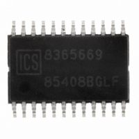
ICS85408BGLF IDT, Integrated Device Technology Inc, ICS85408BGLF Datasheet - Page 4

ICS85408BGLF
Manufacturer Part Number
ICS85408BGLF
Description
IC CLK DISTR DIFF-LVDS 24-TSSOP
Manufacturer
IDT, Integrated Device Technology Inc
Series
HiPerClockS™r
Type
Fanout Buffer (Distribution)r
Datasheet
1.ICS85408BGLF.pdf
(16 pages)
Specifications of ICS85408BGLF
Number Of Circuits
1
Ratio - Input:output
1:8
Differential - Input:output
Yes/Yes
Input
HCSL, LVDS, LVHSTL, LVPECL, SSTL
Output
LVDS
Frequency - Max
700MHz
Voltage - Supply
3.135 V ~ 3.465 V
Operating Temperature
0°C ~ 70°C
Mounting Type
Surface Mount
Package / Case
24-TSSOP
Frequency-max
700MHz
Number Of Outputs
16
Operating Supply Voltage (max)
3.465V
Operating Temp Range
0C to 70C
Propagation Delay Time
5ns
Operating Supply Voltage (min)
3.135V
Mounting
Surface Mount
Pin Count
24
Operating Supply Voltage (typ)
3.3V
Package Type
TSSOP
Duty Cycle
55%
Operating Temperature Classification
Commercial
Lead Free Status / RoHS Status
Lead free / RoHS Compliant
Other names
800-1182
800-1182-5
800-1182
85408BGLF
800-1182-5
800-1182
85408BGLF
Available stocks
Company
Part Number
Manufacturer
Quantity
Price
Part Number:
ICS85408BGLF
Manufacturer:
ICS
Quantity:
20 000
ICS85408 Datasheet
Absolute Maximum Ratings
NOTE: Stresses beyond those listed under Absolute Maximum Ratings may cause permanent damage to the device. These ratings are stress
specifications only. Functional operation of product at these conditions or any conditions beyond those listed in the DC Characteristics or AC
Characteristics is not implied. Exposure to absolute maximum rating conditions for extended periods may affect product reliability.
DC Electrical Characteristics
Table 4A. LVDS Power Supply DC Characteristics,V
Table 4B. LVCMOS/LVTTL DC Characteristics, V
Table 4C. Differential DC Characteristics, V
NOTE 1: V
NOTE 2: Common mode input voltage is defined as V
ICS85408BG REVISION B JUNE 25, 2009
Item
Supply Voltage, V
Inputs, V
Outputs, I
Continuos Current
Surge Current
Package Thermal Impedance, θ
Storage Temperature, T
Symbol
V
I
Symbol
V
V
I
I
Symbol
I
I
V
V
DD
IH
IL
IH
IL
DD
IH
IL
PP
CMR
I
O
IL
Parameter
Input High Current
Input Low Current
Peak-to-Peak Voltage; NOTE 1
Common Mode Input Voltage; NOTE 1, 2
(LVDS)
Parameter
Positive Supply Voltage
Power Supply Current
should not be less than -0.3V.
Parameter
Input High Voltage
Input Low Voltage
Input High Current
Input Low Current
DD
STG
JA
CLK
nCLK
CLK
nCLK
V
DD
DD
V
Test Conditions
Test Conditions
DD
IH
= 3.3V ± 5%, T
= 3.465V, V
.
DD
= V
= 3.3V ± 5%, T
IN
V
V
DD
DD
DD
V
V
= 3.465V
Test Conditions
DD
DD
= 3.3V ± 5%, T
= 3.465V, V
= 3.465V, V
IN
= V
= V
= 0V
4
IN
IN
A
= 0°C to 70°C
= 3.465V
= 3.465V
Rating
4.6V
-0.5V to V
10mA
15mA
70°C/W (0 mps)
-65°C to 150°C
A
IN
IN
= 0°C to 70°C
= 0V
= 0V
LOW SKEW, 1-TO-8, DIFFERENTIAL-TO-LVDS CLOCK DISTRIBUTION CHIP
A
= 0°C to 70°C
DD
Minimum
3.135
+ 0.5V
Minimum
GND + 0.5
Minimum
-150
-0.3
-150
0.15
2
-5
Typical
Typical
3.3
Typical
©2009 Integrated Device Technology, Inc.
Maximum
Maximum
V
V
Maximum
3.465
DD
DD
90
0.8
150
5
1.3
+ 0.3
– 0.85
5
Units
Units
mA
Units
V
µA
µA
V
V
µA
µA
µA
V
V


