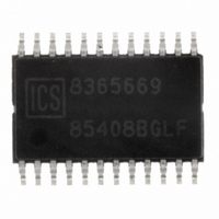
ICS85408BGLF IDT, Integrated Device Technology Inc, ICS85408BGLF Datasheet - Page 2

ICS85408BGLF
Manufacturer Part Number
ICS85408BGLF
Description
IC CLK DISTR DIFF-LVDS 24-TSSOP
Manufacturer
IDT, Integrated Device Technology Inc
Series
HiPerClockS™r
Type
Fanout Buffer (Distribution)r
Datasheet
1.ICS85408BGLF.pdf
(16 pages)
Specifications of ICS85408BGLF
Number Of Circuits
1
Ratio - Input:output
1:8
Differential - Input:output
Yes/Yes
Input
HCSL, LVDS, LVHSTL, LVPECL, SSTL
Output
LVDS
Frequency - Max
700MHz
Voltage - Supply
3.135 V ~ 3.465 V
Operating Temperature
0°C ~ 70°C
Mounting Type
Surface Mount
Package / Case
24-TSSOP
Frequency-max
700MHz
Number Of Outputs
16
Operating Supply Voltage (max)
3.465V
Operating Temp Range
0C to 70C
Propagation Delay Time
5ns
Operating Supply Voltage (min)
3.135V
Mounting
Surface Mount
Pin Count
24
Operating Supply Voltage (typ)
3.3V
Package Type
TSSOP
Duty Cycle
55%
Operating Temperature Classification
Commercial
Lead Free Status / RoHS Status
Lead free / RoHS Compliant
Other names
800-1182
800-1182-5
800-1182
85408BGLF
800-1182-5
800-1182
85408BGLF
Available stocks
Company
Part Number
Manufacturer
Quantity
Price
Part Number:
ICS85408BGLF
Manufacturer:
ICS
Quantity:
20 000
ICS85408 Datasheet
Table 1. Pin Descriptions
NOTE: Pullup and Pulldown refer to internal input resistors. See Table 2, Pin Characteristics, for typical values.
Table 2. Pin Characteristics
Function Tables
Table 3A. Output Enable Function Table
ICS85408BG REVISION B JUNE 25, 2009
Symbol
C
C
R
R
17, 19, 20
IN
PD
PULLUP
PULLDOWN
Number
Inputs
11, 12
13, 14
18, 21
23, 24
9, 10
1, 2
3, 4
5, 6
7, 8
OE
15
16
22
0
1
Parameter
Input Capacitance
Power Dissipation Capacitance
(per output)
Input Pullup Resistor
Input Pulldown Resistor
nQ6, Q6
nQ5, Q5
nQ4, Q4
nQ3, Q3
nQ2, Q2
nQ1, Q1
nQ0, Q0
nQ7, Q7
Name
nCLK
GND
CLK
High-Impedance
V
Q[0:7], nQ[0:7]
OE
Active (default)
DD
Outputs
Output
Output
Output
Output
Output
Output
Output
Output
Power
Power
Input
Input
Input
Type
Pulldown
Pullup
Pullup
Description
Differential output pair. LVDS interface levels.
Differential output pair. LVDS interface levels.
Differential output pair. LVDS interface levels.
Differential output pair. LVDS interface levels.
Differential output pair. LVDS interface levels.
Differential output pair. LVDS interface levels.
Differential output pair. LVDS interface levels.
Inverting differential clock input.
Non-inverting differential clock input.
Positive supply pins.
Power supply ground.
Output enable. Controls the enabling and disabling of outputs Qx, nQx. When HIGH,
the outputs are enabled. When LOW, the outputs are in High-Impedance. LVCMOS /
LVTTL interface levels.
Differential output pair. LVDS interface levels.
Test Conditions
2
LOW SKEW, 1-TO-8, DIFFERENTIAL-TO-LVDS CLOCK DISTRIBUTION CHIP
Minimum
Typical
51
51
4
4
©2009 Integrated Device Technology, Inc.
Maximum
Units
k
k
pF
pF
Ω
Ω


