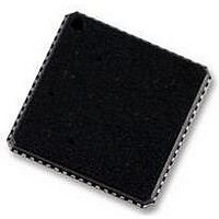
ADSP-BF592KCPZ Analog Devices Inc, ADSP-BF592KCPZ Datasheet - Page 9

ADSP-BF592KCPZ
Manufacturer Part Number
ADSP-BF592KCPZ
Description
58T4522
Manufacturer
Analog Devices Inc
Specifications of ADSP-BF592KCPZ
Operating Temperature (min)
0C
Operating Temperature (max)
70C
Operating Temperature Classification
Commercial
Mounting
Surface Mount
Pin Count
64
Rohs Compliant
YES
Frequency
400MHz
Embedded Interface Type
PPI, SPI, UART
No. Of I/o's
32
Operating Temperature Range
0°C To +70°C
Digital Ic Case Style
LFCSP
No. Of Pins
64
Core Supply Voltage
1.4V
Lead Free Status / RoHS Status
Compliant
Available stocks
Company
Part Number
Manufacturer
Quantity
Price
Company:
Part Number:
ADSP-BF592KCPZ-2
Manufacturer:
BROADCOM
Quantity:
154
Note that when a GPIO pin is used to trigger wake from deep
sleep, the programmed wake level must linger for at least 10ns
to guarantee detection.
Hibernate State—Maximum Static Power Savings
The hibernate state maximizes static power savings by disabling
clocks to the processor core (CCLK) and to all of the peripherals
(SCLK), as well as signaling an external voltage regulator that
V
nally (for example, memory contents, register contents, and
other information) must be written to a nonvolatile storage
device prior to removing power if the processor state is to be
preserved. Writing b#0 to the HIBERNATE bit causes
EXT_WAKE to transition low, which can be used to signal an
external voltage regulator to shut down.
Since V
nal pins three-state, unless otherwise specified. This allows
other devices that may be connected to the processor to still
have power applied without drawing unwanted current.
As long as V
state during hibernation. All other internal registers and memo-
ries, however, lose their content in the hibernate state.
Power Savings
As shown in
power domains, which maximizes flexibility while maintaining
compliance with industry standards and conventions. By isolat-
ing the internal logic of the processor into its own power
domain, separate from other I/O, the processor can take advan-
tage of dynamic power management without affecting the other
I/O devices. There are no sequencing requirements for the
various power domains, but all domains must be powered
according to the appropriate
operating conditions, even if the feature/peripheral is not used.
Table 3. Power Domains
The dynamic power management feature of the processor
allows both the processor’s input voltage (V
quency (f
The power dissipated by a processor is largely a function of its
clock frequency and the square of the operating voltage. For
example, reducing the clock frequency by 25% results in a 25%
reduction in dynamic power dissipation, while reducing the
voltage by 25% reduces dynamic power dissipation by more
than 40%. Further, these power savings are additive, in that if
the clock frequency and supply voltage are both reduced, the
power savings can be dramatic, as shown in the following
equations.
Power Domain
All internal logic and memories
All other I/O
DDINT
can be shut off. Any critical information stored inter-
DDEXT
CCLK
DDEXT
Table
can still be supplied in this mode, all of the exter-
) to be dynamically controlled.
is applied, the VR_CTL register maintains its
3, the processor supports two different
Specifications
table for processor
DDINT
V
V
V
) and clock fre-
DDINT
DDEXT
DD
Rev. A | Page 9 of 44 | August 2011
Range
where:
VOLTAGE REGULATION
The ADSP-BF592 processor requires an external voltage regula-
tor to power the V
consumption, the external voltage regulator can be signaled
through EXT_WAKE to remove power from the processor core.
This signal is high-true for power-up and may be connected
directly to the low-true shut-down input of many common
regulators.
While in the hibernate state, the external supply, V
still be applied, eliminating the need for external buffers. The
external voltage regulator can be activated from this power-
down state by asserting the RESET pin, which then initiates a
boot sequence. EXT_WAKE indicates a wakeup to the external
voltage regulator.
The power good (PG) input signal allows the processor to start
only after the internal voltage has reached a chosen level. In this
way, the startup time of the external regulator is detected after
hibernation. For a complete description of the power-good
functionality, refer to the ADSP-BF59x Blackfin Processor Hard-
ware Reference.
CLOCK SIGNALS
The processor can be clocked by an external crystal, a sine wave
input, or a buffered, shaped clock derived from an external
clock oscillator.
If an external clock is used, it should be a TTL-compatible signal
and must not be halted, changed, or operated below the speci-
fied frequency during normal operation. This signal is
connected to the processor’s CLKIN pin. When an external
clock is used, the XTAL pin must be left unconnected.
Alternatively, because the processor includes an on-chip oscilla-
tor circuit, an external crystal may be used. For fundamental
frequency operation, use the circuit shown in
parallel -resonant, fundamental frequency, microprocessor-
grade crystal is connected across the CLKIN and XTAL pins.
The on-chip resistance between CLKIN and the XTAL pin is in
% Power Savings
Power Savings Factor
=
f
f
V
V
T
T
CCLKNOM
CCLKRED
NOM
RED
DDINTNOM
DDINTRED
------------------- -
f
f
CCLKNOM
CCLKRED
is the duration running at f
is the duration running at f
is the reduced core clock frequency
is the nominal core clock frequency
is the reduced internal supply voltage
is the nominal internal supply voltage
×
------------------------
V
V
=
DDINT
DDINTNOM
DDINTRED
(
1 Power Savings Factor
–
domain. To reduce standby power
2
×
----------- -
T
CCLKRED
T
CCLKNOM
NOM
RED
ADSP-BF592
Figure
)
×
100%
DDEXT
4. A
, can


