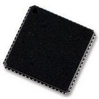
ADSP-BF592KCPZ Analog Devices Inc, ADSP-BF592KCPZ Datasheet - Page 8

ADSP-BF592KCPZ
Manufacturer Part Number
ADSP-BF592KCPZ
Description
58T4522
Manufacturer
Analog Devices Inc
Specifications of ADSP-BF592KCPZ
Operating Temperature (min)
0C
Operating Temperature (max)
70C
Operating Temperature Classification
Commercial
Mounting
Surface Mount
Pin Count
64
Rohs Compliant
YES
Frequency
400MHz
Embedded Interface Type
PPI, SPI, UART
No. Of I/o's
32
Operating Temperature Range
0°C To +70°C
Digital Ic Case Style
LFCSP
No. Of Pins
64
Core Supply Voltage
1.4V
Lead Free Status / RoHS Status
Compliant
Available stocks
Company
Part Number
Manufacturer
Quantity
Price
Company:
Part Number:
ADSP-BF592KCPZ-2
Manufacturer:
BROADCOM
Quantity:
154
ADSP-BF592
General-Purpose Mode Descriptions
The general-purpose modes of the PPI are intended to suit a
wide variety of data capture and transmission applications.
Three distinct submodes are supported:
ITU-R 656 Mode Descriptions
The ITU-R 656 modes of the PPI are intended to suit a wide
variety of video capture, processing, and transmission applica-
tions. Three distinct submodes are supported:
TWI Controller Interface
The processor includes a 2-wire interface (TWI) module for
providing a simple exchange method of control data between
multiple devices. The TWI is functionally compatible with the
widely used I
capabilities of simultaneous master and slave operation and
support for both 7-bit addressing and multimedia data arbitra-
tion. The TWI interface utilizes two pins for transferring clock
(SCL) and data (SDA) and supports the protocol at speeds up to
400K bits/sec.
The TWI module is compatible with serial camera control bus
(SCCB) functionality for easier control of various CMOS cam-
era sensor devices.
Ports
The processor groups the many peripheral signals to two
ports—Port F and Port G. Most of the associated pins are shared
by multiple signals. The ports function as multiplexer controls.
General-Purpose I/O (GPIO)
The processor has 32 bidirectional, general-purpose I/O (GPIO)
pins allocated across two separate GPIO modules—PORTFIO
and PORTGIO, associated with Port F and Port G respectively.
Each GPIO-capable pin shares functionality with other proces-
sor peripherals via a multiplexing scheme; however, the GPIO
functionality is the default state of the device upon power-up.
Neither GPIO output nor input drivers are active by default.
Each general-purpose port pin can be individually controlled by
manipulation of the port control, status, and interrupt registers.
• Input mode – Frame syncs and data are inputs into the PPI.
• Frame capture mode – Frame syncs are outputs from the
• Output mode – Frame syncs and data are outputs from the
• Active video only mode – Active video only mode is used
• Vertical blanking only mode – In this mode, the PPI only
• Entire field mode – In this mode, the entire incoming bit
Input mode is intended for ADC applications, as well as
video communication with hardware signaling.
PPI, but data are inputs. This mode allows the video
source(s) to act as a slave (for frame capture for example).
PPI. Output mode is used for transmitting video or other
data with up to three output frame syncs.
when only the active video portion of a field is of interest
and not any of the blanking intervals.
transfers vertical blanking interval (VBI) data.
stream is read in through the PPI.
2
C
®
bus standard. The TWI module offers the
Rev. A | Page 8 of 44 | August 2011
DYNAMIC POWER MANAGEMENT
The processor provides five operating modes, each with a differ-
ent performance/power profile. In addition, dynamic power
management provides the control functions to dynamically alter
the processor core supply voltage, further reducing power dissi-
pation. When configured for a 0 V core supply voltage, the
processor enters the hibernate state. Control of clocking to each
of the processor peripherals also reduces power consumption.
See
Table 2. Power Settings
Full-On Operating Mode—Maximum Performance
In the full-on mode, the PLL is enabled and is not bypassed,
providing capability for maximum operational frequency. This
is the power-up default execution state in which maximum per-
formance can be achieved. The processor core and all enabled
peripherals run at full speed.
Active Operating Mode—Moderate Dynamic Power
Savings
In the active mode, the PLL is enabled but bypassed. Because the
PLL is bypassed, the processor’s core clock (CCLK) and system
clock (SCLK) run at the input clock (CLKIN) frequency. DMA
access is available to appropriately configured L1 memories.
For more information about PLL controls, see the “Dynamic
Power Management” chapter in the ADSP-BF59x Blackfin Pro-
cessor Hardware Reference.
Sleep Operating Mode—High Dynamic Power Savings
The sleep mode reduces dynamic power dissipation by disabling
the clock to the processor core (CCLK). The PLL and system
clock (SCLK), however, continue to operate in this mode. Typi-
cally, an external event wakes up the processor.
System DMA access to L1 memory is not supported in
sleep mode.
Deep Sleep Operating Mode—Maximum Dynamic Power
Savings
The deep sleep mode maximizes dynamic power savings by dis-
abling the clocks to the processor core (CCLK) and to all
synchronous peripherals (SCLK). Asynchronous peripherals
may still be running but cannot access internal resources or
external memory. This powered-down mode can only be exited
by assertion of the reset interrupt (RESET) or by an asynchro-
nous interrupt generated by a GPIO pin.
Mode/State PLL
Full On
Active
Sleep
Deep Sleep
Hibernate
Table 2
for a summary of the power settings for each mode.
Enabled No
Enabled/
Disabled
Enabled —
Disabled —
Disabled —
PLL
Bypassed
Yes
Core
Clock
(CCLK)
Enabled Enabled On
Enabled Enabled On
Disabled Enabled On
Disabled Disabled On
Disabled Disabled Off
System
Clock
(SCLK)
Core
Power


