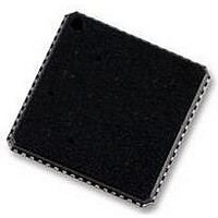
ADSP-BF592KCPZ Analog Devices Inc, ADSP-BF592KCPZ Datasheet - Page 21

ADSP-BF592KCPZ
Manufacturer Part Number
ADSP-BF592KCPZ
Description
58T4522
Manufacturer
Analog Devices Inc
Specifications of ADSP-BF592KCPZ
Operating Temperature (min)
0C
Operating Temperature (max)
70C
Operating Temperature Classification
Commercial
Mounting
Surface Mount
Pin Count
64
Rohs Compliant
YES
Frequency
400MHz
Embedded Interface Type
PPI, SPI, UART
No. Of I/o's
32
Operating Temperature Range
0°C To +70°C
Digital Ic Case Style
LFCSP
No. Of Pins
64
Core Supply Voltage
1.4V
Lead Free Status / RoHS Status
Compliant
Available stocks
Company
Part Number
Manufacturer
Quantity
Price
Company:
Part Number:
ADSP-BF592KCPZ-2
Manufacturer:
BROADCOM
Quantity:
154
TIMING SPECIFICATIONS
Specifications are subject to change without notice.
Clock and Reset Timing
Table 18
the CCLK and SCLK timing specifications in
Table
not select core/peripheral clocks in excess of the processor’s
instruction rate.
Table 18. Clock and Reset Timing
1
2
3
4
5
6
Parameter
Timing Requirements
f
t
t
t
Switching Characteristic
t
Applies to PLL bypass mode and PLL non bypass mode.
Combinations of the CLKIN frequency and the PLL clock multiplier must not exceed the allowed f
The t
If the DF bit in the PLL_CTL register is set, the minimum f
Applies after power-up sequence is complete. See
The ADSP-BF592 processor does not have a dedicated CLKBUF pin. Rather, the EXTCLK pin may be programmed to serve as CLKBUF or CLKOUT. This parameter applies
CKIN
CKINL
CKINH
WRST
BUFDLAY
on Page
when EXTCLK is programmed to output CLKBUF.
CKIN
10, combinations of CLKIN and clock multipliers must
16.
period (see
and
CLKIN Period
CLKIN Low Pulse
CLKIN High Pulse
RESET Asserted Pulse Width Low
CLKIN to CLKBUF
Figure 7
CLKBUF
Figure
CLKIN
describe clock and reset operations. Per
7) equals 1/f
1, 2, 3, 4
1
6
1
Delay
t
CKINL
CKIN
.
t
CKIN
Table 19
t
CKINH
5
Table 8
CKIN
and
Rev. A | Page 21 of 44 | August 2011
specification is 24 MHz.
Figure 8
to
Figure 7. Clock and Reset Timing
Min
12
10
10
11 × t
t
WRST
for power-up reset timing.
CKIN
V
DDEXT
1.8 V Nominal
Max
50
11
VCO
, f
CCLK
, and f
t
BUFDLAY
SCLK
settings discussed in
Min
12
10
10
11 × t
V
CKIN
DDEXT
2.5 V/3.3 V Nominal
Table 8 on Page 16
Max
50
10
t
BUFDLAY
ADSP-BF592
through
Table 10
Unit
MHz
ns
ns
ns
ns


