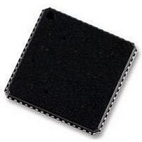
ADSP-BF592KCPZ Analog Devices Inc, ADSP-BF592KCPZ Datasheet - Page 37

ADSP-BF592KCPZ
Manufacturer Part Number
ADSP-BF592KCPZ
Description
58T4522
Manufacturer
Analog Devices Inc
Specifications of ADSP-BF592KCPZ
Operating Temperature (min)
0C
Operating Temperature (max)
70C
Operating Temperature Classification
Commercial
Mounting
Surface Mount
Pin Count
64
Rohs Compliant
YES
Frequency
400MHz
Embedded Interface Type
PPI, SPI, UART
No. Of I/o's
32
Operating Temperature Range
0°C To +70°C
Digital Ic Case Style
LFCSP
No. Of Pins
64
Core Supply Voltage
1.4V
Lead Free Status / RoHS Status
Compliant
Available stocks
Company
Part Number
Manufacturer
Quantity
Price
Company:
Part Number:
ADSP-BF592KCPZ-2
Manufacturer:
BROADCOM
Quantity:
154
The time t
signal switches to when the output voltage reaches V
or V
Time t
when the output reaches the V
voltage.
Time t
If multiple pins are enabled, the measurement value is that of
the first lead to start driving.
Output Disable Time Measurement
Output pins are considered to be disabled when they stop driv-
ing, go into a high impedance state, and start to decay from their
output high or low voltage. The output disable time t
difference between t
side of
The time for the voltage on the bus to decay by ΔV is dependent
on the capacitive load C
time can be approximated by the equation:
The time t
ΔV equal to 0.25 V for V
0.15 V for V
The time t
signal switches to when the output voltage decays ΔV from the
measured output high or output low voltage.
Example System Hold Time Calculation
To determine the data output hold time in a particular system,
first calculate t
to be the difference between the processor’s output voltage and
the input threshold for the device requiring the hold time. C
the total bus capacitance (per data line), and I
age or three-state current (per data line). The hold time will be
t
Timing Specifications on Page
DECAY
• V
• V
• V
TRIP
(low) is 0.75 V
is 1.0 V
is 1.4 V
DDEXT
DDEXT
DDEXT
plus the various output disable times as specified in the
TRIP
ENA
Figure
(low) and is shown below.
ENA_MEASURED
is calculated as shown in the equation:
DECAY
DIS_MEASURED
is the interval from when the output starts driving to
(nominal) = 1.8 V, V
(nominal) = 2.5 V, V
(nominal) = 3.3 V, V
DDEXT
35.
DECAY
t
is calculated with test loads C
DIS
t
(nominal) = 1.8V.
ENA
DIS_MEASURED
using the equation given above. Choose ΔV
=
t
DECAY
is the interval from when the reference
is the interval from when the reference
t
=
DIS_MEASURED
L
DDEXT
and the load current I
t
ENA_MEASURED
=
(nominal) = 2.5 V/3.3 V and
TRIP
21.
(
and t
C
TRIP
TRIP
TRIP
(high) or V
L
Δ
–
V
(high) is 1.05 V, V
(high) is 1.5 V, V
(high) is 1.9 V, V
DECAY
t
) I
DECAY
–
⁄
t
L
TRIP
as shown on the left
TRIP
L
L
and I
is the total leak-
L
. This decay
(low) trip
Rev. A | Page 37 of 44 | August 2011
L
TRIP
, and with
DIS
TRIP
TRIP
TRIP
(high)
is the
(low)
(low)
L
is
Capacitive Loading
Output delays and holds are based on standard capacitive loads
of an average of 6 pF on all pins (see
to (V
The graphs of
rise time varies with capacitance. The delay and hold specifica-
tions given should be derated by a factor derived from these
figures. The graphs in these figures may not be linear outside the
ranges shown.
NOTES:
THE WORST CASE TRANSMISSION LINE DELAY IS SHOWN AND CAN BE USED
FOR THE OUTPUT TIMING ANALYSIS TO REFELECT THE TRANSMISSION LINE
EFFECT AND MUST BE CONSIDERED. THE TRANSMISSION LINE (TD) IS FOR
LOAD ONLY AND DOES NOT AFFECT THE DATA SHEET TIMING SPECIFICATIONS.
ANALOG DEVICES RECOMMENDS USING THE IBIS MODEL TIMING FOR A GIVEN
SYSTEM REQUIREMENT. IF NECESSARY, A SYSTEM MAY INCORPORATE
EXTERNAL DRIVERS TO COMPENSATE FOR ANY TIMING DIFFERENCES.
V
LOAD
20
18
16
14
12
10
4pF
Figure 37. Driver Type A Typical Rise and Fall Times (10%–90%) vs.
8
6
4
2
0
DDEXT
0
Figure 36. Equivalent Device Loading for AC Measurements
50:
)/2.
Figure 37
70:
50:
400:
2pF
50
Load Capacitance (1.8V V
TESTER PIN ELECTRONICS
through
(Includes All Fixtures)
45:
0.5pF
LOAD CAPACITANCE (pF)
100
Figure 42
Figure
ZO = 50: (impedance)
TD = 4.04 r 1.18 ns
150
DDEXT
t
show how output
FALL
ADSP-BF592
T1
36). V
)
t
t
FALL
RISE
= 1.8V @ 25
= 1.8V @ 25
t
RISE
LOAD
200
is equal
OUTPUT
DUT
° C
° C
250


