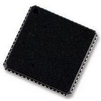
ADSP-BF592KCPZ Analog Devices Inc, ADSP-BF592KCPZ Datasheet - Page 10

ADSP-BF592KCPZ
Manufacturer Part Number
ADSP-BF592KCPZ
Description
58T4522
Manufacturer
Analog Devices Inc
Specifications of ADSP-BF592KCPZ
Operating Temperature (min)
0C
Operating Temperature (max)
70C
Operating Temperature Classification
Commercial
Mounting
Surface Mount
Pin Count
64
Rohs Compliant
YES
Frequency
400MHz
Embedded Interface Type
PPI, SPI, UART
No. Of I/o's
32
Operating Temperature Range
0°C To +70°C
Digital Ic Case Style
LFCSP
No. Of Pins
64
Core Supply Voltage
1.4V
Lead Free Status / RoHS Status
Compliant
Available stocks
Company
Part Number
Manufacturer
Quantity
Price
Company:
Part Number:
ADSP-BF592KCPZ-2
Manufacturer:
BROADCOM
Quantity:
154
ADSP-BF592
the 500 kΩ range. Further parallel resistors are typically not rec-
ommended. The two capacitors and the series resistor shown in
Figure 4
The capacitor and resistor values shown in
values only. The capacitor values are dependent upon the crystal
manufacturers’ load capacitance recommendations and the PCB
physical layout. The resistor value depends on the drive level
specified by the crystal manufacturer. The user should verify the
customized values based on careful investigations on multiple
devices over temperature range.
A third-overtone crystal can be used for frequencies above
25 MHz. The circuit is then modified to ensure crystal operation
only at the third overtone, by adding a tuned inductor circuit as
shown in
ation is discussed in detail in (EE-168) Using Third Overtone
Crystals with the ADSP-218x DSP on the Analog Devices web-
site (www.analog.com)—use site search on “EE-168.”
The Blackfin core runs at a different clock rate than the on-chip
peripherals. As shown in
system peripheral clock (SCLK) are derived from the input
clock (CLKIN) signal. An on-chip PLL is capable of multiplying
the CLKIN signal by a programmable 5× to 64× multiplication
factor (bounded by specified minimum and maximum VCO
frequencies). The default multiplier is 6×, but it can be modified
by a software instruction sequence.
On-the-fly frequency changes can be effected by simply writing
to the PLL_DIV register. The maximum allowed CCLK and
SCLK rates depend on the applied voltages V
the VCO is always permitted to run up to the frequency speci-
fied by the part’s instruction rate. The EXTCLK pin can be
configured to output either the SCLK frequency or the input
buffered CLKIN frequency, called CLKBUF. When configured
to output SCLK (CLKOUT), the EXTCLK pin acts as a refer-
ence signal in many timing specifications. While three-stated by
default, it can be enabled using the VRCTL register.
EXTCLK
NOTE: VALUES MARKED WITH * MUST BE CUSTOMIZED, DEPENDING
ON THE CRYSTAL AND LAYOUT. PLEASE ANALYZE CAREFULLY. FOR
FREQUENCIES ABOVE 33 MHz, THE SUGGESTED CAPACITOR VALUE
OF 18 pF SHOULD BE TREATED AS A MAXIMUM, AND THE SUGGESTED
RESISTOR VALUE SHOULD BE REDUCED TO 0
EN
fine tune phase and amplitude of the sine frequency.
Figure
SELECT
Figure 4. External Crystal Connections
4. A design procedure for third-overtone oper-
EN
BLACKFIN
CLKBUF
CLKIN
Figure
18 pF *
330
TO PLL CIRCUITRY
5, the core clock (CCLK) and
CLKOUT (SCLK)
*
560
XTAL
18 pF *
.
Figure 4
FOR OVERTONE
OPERATION ONLY:
DDINT
and V
Rev. A | Page 10 of 44 | August 2011
are typical
DDEXT
;
All on-chip peripherals are clocked by the system clock (SCLK).
The system clock frequency is programmable by means of the
SSEL3–0 bits of the PLL_DIV register. The values programmed
into the SSEL fields define a divide ratio between the PLL output
(VCO) and the system clock. SCLK divider values are 1 through
15.
Note that the divisor ratio must be chosen to limit the system
clock frequency to its maximum of f
changed dynamically without any PLL lock latencies by writing
the appropriate values to the PLL divisor register (PLL_DIV).
The core clock (CCLK) frequency can also be dynamically
changed by means of the CSEL1–0 bits of the PLL_DIV register.
Supported CCLK divider ratios are 1, 2, 4, and 8, as shown in
Table
fast core frequency modifications.
Table 5. Core Clock Ratios
Table 4. Example System Clock Ratios
The maximum CCLK frequency both depends on the part’s
instruction rate (see Page
V
clock rate (SCLK) depends on the chip package and the applied
V
Signal Name
CSEL1–0
00
01
10
11
Signal Name
SSEL3–0
0010
0110
1010
CLKIN
DDINT
DDINT
Table 4
5. This programmable core clock capability is useful for
voltage. See
and V
REQUIRES PLL SEQUENCING
“FINE” ADJUSTMENT
illustrates typical system clock ratios.
5u to 64u
DDEXT
Figure 5. Frequency Modification Methods
PLL
Divider Ratio
VCO/CCLK
1:1
2:1
4:1
8:1
Divider Ratio
VCO/SCLK
2:1
6:1
10:1
voltages (see
Table 8
Page
for details. The maximal system
SCLK d CCLK
VCO
43) and depends on the applied
Table
VCO
300
300
400
200
VCO
100
300
400
Example Frequency Ratios
Example Frequency Ratios
SCLK
“COARSE” ADJUSTMENT
10).
÷ 1 to 15
÷ 1, 2, 4, 8
. The SSEL value can be
ON-THE-FLY
(MHz)
(MHz)
CCLK
300
150
100
25
SCLK
50
50
40
CCLK
SCLK


