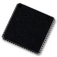
ADSP-BF592KCPZ Analog Devices Inc, ADSP-BF592KCPZ Datasheet - Page 5

ADSP-BF592KCPZ
Manufacturer Part Number
ADSP-BF592KCPZ
Description
58T4522
Manufacturer
Analog Devices Inc
Specifications of ADSP-BF592KCPZ
Operating Temperature (min)
0C
Operating Temperature (max)
70C
Operating Temperature Classification
Commercial
Mounting
Surface Mount
Pin Count
64
Rohs Compliant
YES
Frequency
400MHz
Embedded Interface Type
PPI, SPI, UART
No. Of I/o's
32
Operating Temperature Range
0°C To +70°C
Digital Ic Case Style
LFCSP
No. Of Pins
64
Core Supply Voltage
1.4V
Lead Free Status / RoHS Status
Compliant
Available stocks
Company
Part Number
Manufacturer
Quantity
Price
Company:
Part Number:
ADSP-BF592KCPZ-2
Manufacturer:
BROADCOM
Quantity:
154
MEMORY ARCHITECTURE
The Blackfin processor views memory as a single unified
4G byte address space, using 32-bit addresses. All resources,
including internal memory and I/O control registers, occupy
separate sections of this common address space. See
The core-accessible L1 memory system is high performance
internal memory that operates at the core clock frequency. The
external bus interface unit (EBIU) provides access to the boot
ROM.
The memory DMA controller provides high bandwidth data-
movement capability. It can perform block transfers of code or
data between the L1 Instruction SRAM and L1 Data SRAM
memory spaces.
Internal (Core-Accessible) Memory
The processor has three blocks of core-accessible memory, pro-
viding high bandwidth access to the core.
The first block is the L1 instruction memory, consisting of
32K bytes SRAM. This memory is accessed at full processor
speed.
The second core-accessible memory block is the L1 data mem-
ory, consisting of 32K bytes. This memory block is accessed at
full processor speed.
The third memory block is a 4K byte L1 scratchpad SRAM,
which runs at the same speed as the other L1 memories.
L1 Utility ROM
The L1 instruction ROM contains utility ROM code. This
includes the TMK (VDK core), C run-time libraries, and DSP
libraries. See the VisualDSP++ documentation for more
information.
0xFFFF FFFF
0xFFE0 0000
0xFFC0 0000
0xFFB0 1000
0xFFB0 0000
0xFFA2 0000
0xFFA1 0000
0xFFA0 8000
0xFFA0 4000
0xFFA0 0000
0xFF80 8000
0xFF80 0000
0xEF00 1000
0xEF00 0000
0x0000 0000
Figure 3. Internal/External Memory Map
SYSTEM MEMORY MAPPED REGISTERS (2M BYTES)
CORE MEMORY MAPPED REGISTERS (2M BYTES)
L1 INSTRUCTION BANK B SRAM (16K BYTES)
L1 INSTRUCTION BANK A SRAM (16K BYTES)
L1 INSTRUCTION ROM (64K BYTES)
L1 SCRATCHPAD RAM (4K BYTES)
DATA SRAM (32K BYTES)
BOOT ROM (4K BYTES)
RESERVED
RESERVED
RESERVED
RESERVED
RESERVED
RESERVED
Rev. A | Page 5 of 44 | August 2011
Figure
3.
Custom ROM (Optional)
The on-chip L1 Instruction ROM on the ADSP-BF592 may be
customized to contain user code with the following features:
Customers wishing to customize the on-chip ROM for their
own application needs should contact ADI sales for more infor-
mation on terms and conditions and details on the technical
implementation.
I/O Memory Space
The processor does not define a separate I/O space. All
resources are mapped through the flat 32-bit address space.
On-chip I/O devices have their control registers mapped into
memory-mapped registers (MMRs) at addresses near the top of
the 4G byte address space. These are separated into two smaller
blocks, one which contains the control MMRs for all core func-
tions, and the other which contains the registers needed for
setup and control of the on-chip peripherals outside of the core.
The MMRs are accessible only in supervisor mode and appear
as reserved space to on-chip peripherals.
Booting from ROM
The processor contains a small on-chip boot kernel, which con-
figures the appropriate peripheral for booting. If the processor is
configured to boot from boot ROM memory space, the proces-
sor starts executing from the on-chip boot ROM. For more
information, see
EVENT HANDLING
The event controller on the processor handles all asynchronous
and synchronous events to the processor. The processor
provides event handling that supports both nesting and prioriti-
zation. Nesting allows multiple event service routines to be
active simultaneously. Prioritization ensures that servicing of a
higher-priority event takes precedence over servicing of a lower-
priority event. The controller provides support for five different
types of events:
• 64K bytes of L1 Instruction ROM available for custom code
• Ability to restrict access to all or specific segments of the
• Emulation – An emulation event causes the processor to
• RESET – This event resets the processor.
• Nonmaskable Interrupt (NMI) – The NMI event can be
on-chip ROM
enter emulation mode, allowing command and control of
the processor via the JTAG interface.
generated by the software watchdog timer or by the NMI
input signal to the processor. The NMI event is frequently
used as a power-down indicator to initiate an orderly shut-
down of the system.
Booting Modes on Page
11.
ADSP-BF592


