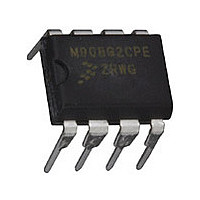
MC68HC908QT2CPE Freescale, MC68HC908QT2CPE Datasheet - Page 148

MC68HC908QT2CPE
Manufacturer Part Number
MC68HC908QT2CPE
Description
Manufacturer
Freescale
Datasheet
1.MC68HC908QT2CPE.pdf
(184 pages)
Specifications of MC68HC908QT2CPE
Cpu Family
HC08
Device Core Size
8b
Frequency (max)
8MHz
Total Internal Ram Size
128Byte
# I/os (max)
6
Number Of Timers - General Purpose
2
Operating Supply Voltage (typ)
3.3/5V
Operating Supply Voltage (max)
5.5V
Operating Supply Voltage (min)
2.7V
On-chip Adc
4-chx8-bit
Instruction Set Architecture
CISC
Operating Temp Range
-40C to 85C
Operating Temperature Classification
Industrial
Mounting
Through Hole
Pin Count
8
Package Type
PDIP
Program Memory Type
Flash
Program Memory Size
1.5KB
Lead Free Status / RoHS Status
Compliant
- Current page: 148 of 184
- Download datasheet (2Mb)
Development Support
15.3.2 Security
A security feature discourages unauthorized reading of FLASH locations while in monitor mode. The host
can bypass the security feature at monitor mode entry by sending eight security bytes that match the
bytes at locations $FFF6–$FFFD. Locations $FFF6–$FFFD contain user-defined data.
During monitor mode entry, the MCU waits after the power-on reset for the host to send the eight security
bytes on pin PTA0. If the received bytes match those at locations $FFF6–$FFFD, the host bypasses the
security feature and can read all FLASH locations and execute code from FLASH. Security remains
bypassed until a power-on reset occurs. If the reset was not a power-on reset, security remains bypassed
and security code entry is not required. See
Upon power-on reset, if the received bytes of the security code do not match the data at locations
$FFF6–$FFFD, the host fails to bypass the security feature. The MCU remains in monitor mode, but
reading a FLASH location returns an invalid value and trying to execute code from FLASH causes an
illegal address reset. After receiving the eight security bytes from the host, the MCU transmits a break
character, signifying that it is ready to receive a command.
To determine whether the security code entered is correct, check to see if bit 6 of RAM address $80 is
set. If it is, then the correct security code has been entered and FLASH can be accessed.
If the security sequence fails, the device should be reset by a power-on reset and brought up in monitor
mode to attempt another entry. After failing the security sequence, the FLASH module can also be mass
erased by executing an erase routine that was downloaded into internal RAM. The mass erase operation
clears the security code locations so that all eight security bytes become $FF (blank).
148
Notes:
1 = Echo delay, 2 bit times
2 = Data return delay, 2 bit times
4 = Wait 1 bit time before sending next byte.
Do not leave locations $FFF6–$FFFD blank. For security reasons, program
locations $FFF6–$FFFD even if they are not used for vectors.
The MCU does not transmit a break character until after the host sends the
eight security bytes.
V
RST
PA0
DD
256 BUS CYCLES
Figure 15-18. Monitor Mode Entry Timing
FROM HOST
(MINIMUM)
MC68HC908QY/QT Family Data Sheet, Rev. 6
4096 + 32 CGMXCLK CYCLES
FROM MCU
Figure
1
NOTE
NOTE
15-18.
4
1
1
2
4
Freescale Semiconductor
1
Related parts for MC68HC908QT2CPE
Image
Part Number
Description
Manufacturer
Datasheet
Request
R

Part Number:
Description:
TOWER ELEVATOR BOARDS HARDWARE
Manufacturer:
Freescale Semiconductor
Datasheet:

Part Number:
Description:
TOWER SERIAL I/O HARDWARE
Manufacturer:
Freescale Semiconductor
Datasheet:

Part Number:
Description:
LCD MODULE FOR TWR SYSTEM
Manufacturer:
Freescale Semiconductor
Datasheet:

Part Number:
Description:
DAUGHTER LCD WVGA I.MX51
Manufacturer:
Freescale Semiconductor
Datasheet:

Part Number:
Description:
TOWER SYSTEM BOARD MPC5125
Manufacturer:
Freescale Semiconductor
Datasheet:

Part Number:
Description:
KIT EVALUATION I.MX51
Manufacturer:
Freescale Semiconductor
Datasheet:

Part Number:
Description:
KIT DEVELOPMENT WINCE IMX25
Manufacturer:
Freescale Semiconductor
Datasheet:

Part Number:
Description:
TOWER SYSTEM KIT MPC5125
Manufacturer:
Freescale Semiconductor
Datasheet:

Part Number:
Description:
TOWER SYSTEM BOARD K40X256
Manufacturer:
Freescale Semiconductor
Datasheet:

Part Number:
Description:
TOWER SYSTEM KIT K40X256
Manufacturer:
Freescale Semiconductor
Datasheet:

Part Number:
Description:
Microcontrollers (MCU) MX28 PLATFORM DEV KIT
Manufacturer:
Freescale Semiconductor
Datasheet:

Part Number:
Description:
MCU, MPU & DSP Development Tools IAR KickStart Kit for Kinetis K60
Manufacturer:
Freescale Semiconductor
Datasheet:

Part Number:
Description:
24BIT HDMI MX535/08
Manufacturer:
Freescale Semiconductor
Datasheet:
Part Number:
Description:
Manufacturer:
Freescale Semiconductor, Inc
Datasheet:
Part Number:
Description:
Manufacturer:
Freescale Semiconductor, Inc
Datasheet:


